- 您现在的位置:买卖IC网 > PDF目录98145 > ST72344S2T6TR (STMICROELECTRONICS) MICROCONTROLLER, PQFP44 PDF资料下载
参数资料
| 型号: | ST72344S2T6TR |
| 厂商: | STMICROELECTRONICS |
| 元件分类: | 微控制器/微处理器 |
| 英文描述: | MICROCONTROLLER, PQFP44 |
| 封装: | 10 X 10 MM, ROHS COMPLIANT, TQFP-32 |
| 文件页数: | 123/246页 |
| 文件大小: | 2016K |
| 代理商: | ST72344S2T6TR |
第1页第2页第3页第4页第5页第6页第7页第8页第9页第10页第11页第12页第13页第14页第15页第16页第17页第18页第19页第20页第21页第22页第23页第24页第25页第26页第27页第28页第29页第30页第31页第32页第33页第34页第35页第36页第37页第38页第39页第40页第41页第42页第43页第44页第45页第46页第47页第48页第49页第50页第51页第52页第53页第54页第55页第56页第57页第58页第59页第60页第61页第62页第63页第64页第65页第66页第67页第68页第69页第70页第71页第72页第73页第74页第75页第76页第77页第78页第79页第80页第81页第82页第83页第84页第85页第86页第87页第88页第89页第90页第91页第92页第93页第94页第95页第96页第97页第98页第99页第100页第101页第102页第103页第104页第105页第106页第107页第108页第109页第110页第111页第112页第113页第114页第115页第116页第117页第118页第119页第120页第121页第122页当前第123页第124页第125页第126页第127页第128页第129页第130页第131页第132页第133页第134页第135页第136页第137页第138页第139页第140页第141页第142页第143页第144页第145页第146页第147页第148页第149页第150页第151页第152页第153页第154页第155页第156页第157页第158页第159页第160页第161页第162页第163页第164页第165页第166页第167页第168页第169页第170页第171页第172页第173页第174页第175页第176页第177页第178页第179页第180页第181页第182页第183页第184页第185页第186页第187页第188页第189页第190页第191页第192页第193页第194页第195页第196页第197页第198页第199页第200页第201页第202页第203页第204页第205页第206页第207页第208页第209页第210页第211页第212页第213页第214页第215页第216页第217页第218页第219页第220页第221页第222页第223页第224页第225页第226页第227页第228页第229页第230页第231页第232页第233页第234页第235页第236页第237页第238页第239页第240页第241页第242页第243页第244页第245页第246页
ST72344xx, ST72345xx
Electrical characteristics
209/246
13.6.1
Crystal and ceramic resonator oscillators
The ST7 internal clock can be supplied with four different Crystal/Ceramic resonator
oscillators. All the information given in this paragraph is based on characterization results
with specified typical external components. In the application, the resonator and the load
capacitors have to be placed as close as possible to the oscillator pins in order to minimize
output distortion and startup stabilization time. Refer to the crystal/ceramic resonator
manufacturer for more details (frequency, package, accuracy, etc.).
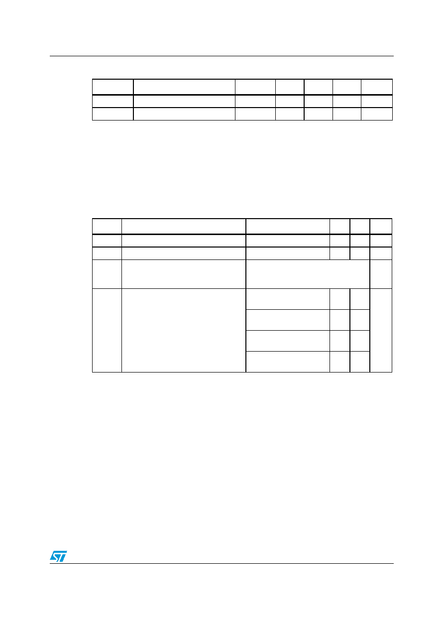
Table 96.
Auto-wakeup from Halt oscillator (AWU) characteristics
Symbol
Parameter
Conditions
Min
Typ
Max
Unit
fAWU
AWU oscillator frequency
50
125
250
kHz
tRCSRT
AWU oscillator startup time
50
s
Table 97.
Crystal/ceramic resonator oscillator characteristics
Symbol
Parameter
Conditions
Min
Max
Unit
fOSC
Oscillator frequency (1)
1.
The oscillator selection can be optimized in terms of supply current using an high quality resonator with
small RS value. Refer to crystal/ceramic resonator manufacturer for more details.
116
MHz
RF
Feedback resistor(2)
2.
Data based on characterisation results, not tested in production. The relatively low value of the RF
resistor, offers a good protection against issues resulting from use in a humid environment, due to the
induced leakage and the bias condition change. However, it is recommended to take this point into
account if the C is used in tough humidity conditions.
20
40
k
Ω
CL1
CL2
Recommended load capacitance versus
equivalent serial resistance of the
crystal or ceramic resonator (RS)
(3)
3.
For CL1 and CL2 it is recommended to use high-quality ceramic capacitors in the 5-pF to 25-pF range (typ.)
designed for high-frequency applications and selected to match the requirements of the crystal or
resonator. CL1 and CL2, are usually the same size. The crystal manufacturer typically specifies a load
capacitance which is the series combination of CL1 and CL2. PCB and MCU pin capacitance must be
included when sizing CL1 and CL2 (10 pF can be used as a rough estimate of the combined pin and board
capacitance).
See Table 98 below
pF
i2
OSC2 driving current
fOSC= 2 MHz, C0 = 6 pF,
CL1 = CL2 = 68 pF
426
A
fOSC= 4 MHz, C0 = 6 pF,
CL1 = CL2 = 68 pF
425
fOSC= 8 MHz, C0 = 6 pF,
CL1 = CL2 = 40 pF
456
fOSC= 16 MHz, C0 = 7 pF,
CL1 = CL2 = 20 pF
660
相关PDF资料 |
PDF描述 |
|---|---|
| ST72344S4T6 | MICROCONTROLLER, PQFP44 |
| ST72345C4T6TR | MICROCONTROLLER, PQFP48 |
| ST72521AR7T1/XXX | 8-BIT, MROM, 8 MHz, MICROCONTROLLER, PQFP64 |
| ST72521R7T5/XXX | 8-BIT, MROM, 8 MHz, MICROCONTROLLER, PQFP64 |
| ST72521AR7TC/XXX | 8-BIT, MROM, 8 MHz, MICROCONTROLLER, PQFP64 |
相关代理商/技术参数 |
参数描述 |
|---|---|
| ST72345 | 制造商:STMICROELECTRONICS 制造商全称:STMicroelectronics 功能描述:8-BIT MCU WITH UP TO 16K FLASH MEMORY, 10-BIT ADC, TWO 16-BIT TIMERS, TWO I2C, SPI, SCI |
| ST72345-D/RAIS | 功能描述:子卡和OEM板 8 BITS MICROCONTR RoHS:否 制造商:BeagleBoard by CircuitCo 产品:BeagleBone LCD4 Boards 用于:BeagleBone - BB-Bone - Open Source Development Kit |
| ST72361 | 制造商:STMICROELECTRONICS 制造商全称:STMicroelectronics 功能描述:8-bit MCU with Flash or ROM, 10-bit ADC, 5 timers, SPI, 2x LINSCI⑩ |
| ST72361_07 | 制造商:STMICROELECTRONICS 制造商全称:STMicroelectronics 功能描述:8-bit MCU with Flash or ROM, 10-bit ADC, 5 timers, SPI, 2x LINSCI⑩ |
| ST72361K6T6 | 制造商:STMicroelectronics 功能描述:ROMLESS MICRO WITH 2 UART - Bulk |
发布紧急采购,3分钟左右您将得到回复。