- 您现在的位置:买卖IC网 > PDF目录66260 > ST72651AR6T1 (STMICROELECTRONICS) 8-BIT, MROM, 8 MHz, MICROCONTROLLER, PQFP64 PDF资料下载
参数资料
| 型号: | ST72651AR6T1 |
| 厂商: | STMICROELECTRONICS |
| 元件分类: | 微控制器/微处理器 |
| 英文描述: | 8-BIT, MROM, 8 MHz, MICROCONTROLLER, PQFP64 |
| 封装: | 10 X 10 MM, TQFP-64 |
| 文件页数: | 6/9页 |
| 文件大小: | 70K |
| 代理商: | ST72651AR6T1 |
ST7265
6/9
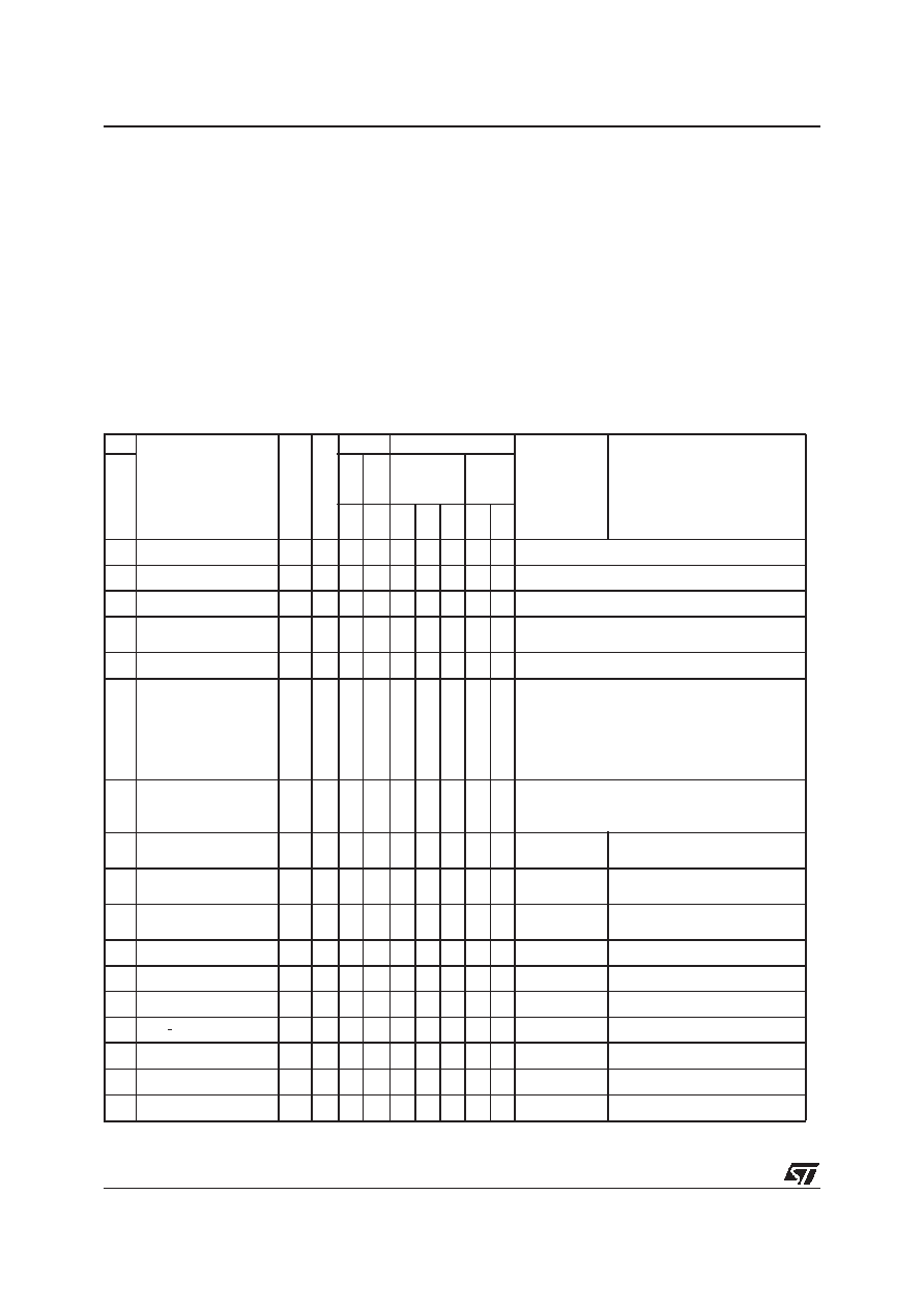
PIN DESCRIPTION (Cont’d)
Legend / Abbreviations:
Type: I = input, O = output, S = supply
VDDF powered: I/O powered by the alternate sup-
ply rail, supplied by VDDF and VSSF.
In/Output level: CT = CMOS 0.3VDD/0.7VDD with
input trigger
Output level: HS = 10mA high sink (on N-buffer
only)
Port and control configuration:
– Input:float = floating, wpu = weak pull-up, int = in-
terrupt
– Output: OD = open drain, T = true open drain, PP
= push-pull, OP = pull-up enabled by option byte.
Refer to “I/O Port Implementation” on page 51 of
the datasheet for more details on the software
configuration of the
I/O ports.
The RESET configuration of each pin is shown in
bold.
Table 1. Device Pin Description
Pin
Pin Name
Type
V
DDF
Powered
Level
Port / Control
Main
Function
(after reset)
Alternate Function
TQFP64
Input
Output
Input
Output
float
wpu
int
OD
PP
1
USBVSS
S
USB Digital ground
2
USBDM
I/O
USB bidirectional data (data -)
3
USBDP
I/O
USB bidirectional data (data +)
4
USBVCC
O
USB power supply, output by the on-chip USB
3.3V linear regulator.
5
USBVDD
S
USB Power supply voltage (4V - 5.5V)
6VDDF
SX
Power Line for alternate supply rail. Can be
used as input (with external supply) or output
(when using the on-chip voltage regulator).
Note: An external decoupling capacitor (min.
20nF) must be connected to this pin to stabilize
the regulator.
7VSSF
SX
Ground Line for alternate supply rail. Can be
used as input (with external supply) or output
(when using the on-chip voltage regulator)
8
PE5/DTC
I/O
X
CT HS X
2
X2
X
Port E5
DTC I/O with serial capability
(MMC_CMD)
9
PE6/DTC
I/O
X
CT HS X
X
Port E6
DTC I/O with serial capability
(MMC_DAT)
10
PE7/DTC
I/O
X
CT HS X
X
Port E7
DTC I/O with serial capability
(MMC_CLK)
11
PB0/DTC
I/O
X CT
X
Port B0
DTC
12
PB1/DTC
I/O
X CT
X
Port B1
DTC
13
PB2/DTC
I/O
X CT
X
Port B2
DTC
14
PB3/DTC
I/O
X CT
X
Port B3
DTC
15
PB4/DTC
I/O
X CT
X
Port B4
DTC
16
PB5/DTC
I/O
X CT
X
Port B5
DTC
17
PB6/DTC
I/O
X CT
X
Port B6
DTC
1
相关PDF资料 |
PDF描述 |
|---|---|
| ST72652R6T1 | 8-BIT, MROM, 8 MHz, MICROCONTROLLER, PQFP64 |
| ST72651AR4T1 | 8-BIT, MROM, 8 MHz, MICROCONTROLLER, PQFP64 |
| ST72652R4T1 | 8-BIT, MROM, 8 MHz, MICROCONTROLLER, PQFP64 |
| ST72F651R6T1 | 8-BIT, FLASH, MICROCONTROLLER, PQFP64 |
| ST72F651R6T1E | 8-BIT, FLASH, MICROCONTROLLER, PQFP64 |
相关代理商/技术参数 |
参数描述 |
|---|---|
| ST7265X-EVAL/MS | 制造商:STMicroelectronics 功能描述:ST6 EVAL BD - Bulk |
| ST7265X-EVAL/PFD | 制造商:STMicroelectronics 功能描述:USB FLASH EVAL - Bulk |
| ST7266 | 制造商:6940 功能描述:ST7266 |
| ST7267C8T1L | 制造商:STMicroelectronics 功能描述: |
| ST72681/R12 | 制造商:STMicroelectronics 功能描述:CONTROLLER FOR HIGH-PERFORMANCE BUS-POWERED USB 2.0 FLASH DR - Trays |
发布紧急采购,3分钟左右您将得到回复。