- 您现在的位置:买卖IC网 > PDF目录69366 > ST72C215G2M7 (STMICROELECTRONICS) 8-BIT, FLASH, 8 MHz, MICROCONTROLLER, PDSO28 PDF资料下载
参数资料
| 型号: | ST72C215G2M7 |
| 厂商: | STMICROELECTRONICS |
| 元件分类: | 微控制器/微处理器 |
| 英文描述: | 8-BIT, FLASH, 8 MHz, MICROCONTROLLER, PDSO28 |
| 封装: | 0.300 INCH, PLASTIC, SOIC-28 |
| 文件页数: | 69/140页 |
| 文件大小: | 2246K |
| 代理商: | ST72C215G2M7 |
第1页第2页第3页第4页第5页第6页第7页第8页第9页第10页第11页第12页第13页第14页第15页第16页第17页第18页第19页第20页第21页第22页第23页第24页第25页第26页第27页第28页第29页第30页第31页第32页第33页第34页第35页第36页第37页第38页第39页第40页第41页第42页第43页第44页第45页第46页第47页第48页第49页第50页第51页第52页第53页第54页第55页第56页第57页第58页第59页第60页第61页第62页第63页第64页第65页第66页第67页第68页当前第69页第70页第71页第72页第73页第74页第75页第76页第77页第78页第79页第80页第81页第82页第83页第84页第85页第86页第87页第88页第89页第90页第91页第92页第93页第94页第95页第96页第97页第98页第99页第100页第101页第102页第103页第104页第105页第106页第107页第108页第109页第110页第111页第112页第113页第114页第115页第116页第117页第118页第119页第120页第121页第122页第123页第124页第125页第126页第127页第128页第129页第130页第131页第132页第133页第134页第135页第136页第137页第138页第139页第140页
ST72104G, ST72215G, ST72216G, ST72254G
34/140
I/O PORTS (Cont’d)
9.4 LOW POWER MODES
9.5 INTERRUPTS
The external interrupt event generates an interrupt
if the corresponding configuration is selected with
DDR and OR registers and the I-bit in the CC reg-
ister is reset (RIM instruction).
9.6 REGISTER DESCRIPTION
DATA REGISTER (DR)
Port x Data Register
PxDR with x = A, B or C.
Read/Write
Reset Value: 0000 0000 (00h)
Bit 7:0 = D[7:0] Data register 8 bits.
The DR register has a specific behaviour accord-
ing to the selected input/output configuration. Writ-
ing the DR register is always taken into account
even if the pin is configured as an input; this allows
always having the expected level on the pin when
toggling to output mode. Reading the DR register
returns either the DR register latch content (pin
configured as output) or the digital value applied to
the I/O pin (pin configured as input).
DATA DIRECTION REGISTER (DDR)
Port x Data Direction Register
PxDDR with x = A, B or C.
Read/Write
Reset Value: 0000 0000 (00h)
Bit 7:0 = DD[7:0] Data direction register 8 bits.
The DDR register gives the input/output direction
configuration of the pins. Each bit is set and
cleared by software.
0: Input mode
1: Output mode
OPTION REGISTER (OR)
Port x Option Register
PxOR with x = A, B or C.
Read/Write
Reset Value: 0000 0000 (00h)
Bit 7:0 = O[7:0] Option register 8 bits.
For specific I/O pins, this register is not implement-
ed. In this case the DDR register is enough to se-
lect the I/O pin configuration.
The OR register allows to distinguish: in input
mode if the pull-up with interrupt capability or the
basic pull-up configuration is selected, in output
mode if the push-pull or open drain configuration is
selected.
Each bit is set and cleared by software.
Input mode:
0: Floating input
1: Pull-up input with or without interrupt
Output mode:
0: Output open drain (with P-Buffer deactivated)
1: Output push-pull (when available)
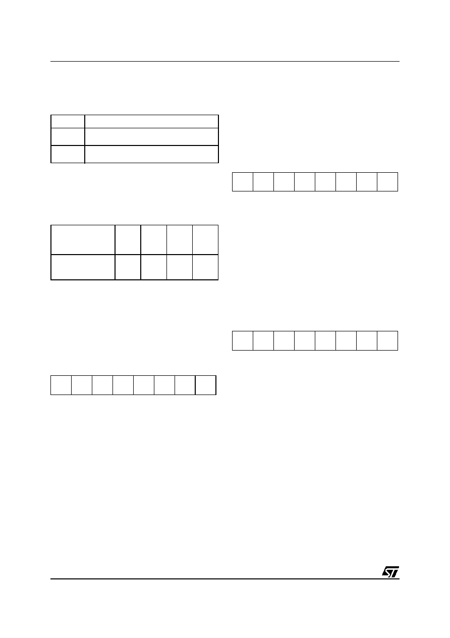
Mode
Description
WAIT
No effect on I/O ports. External interrupts
cause the device to exit from WAIT mode.
HALT
No effect on I/O ports. External interrupts
cause the device to exit from HALT mode.
Interrupt Event
Event
Flag
Enable
Control
Bit
Exit
from
Wait
Exit
from
Halt
External interrupt on
selected external
event
-
DDRx
ORx
Yes
70
D7
D6
D5
D4
D3
D2
D1
D0
70
DD7
DD6
DD5
DD4
DD3
DD2
DD1
DD0
70
O7
O6
O5
O4
O3
O2
O1
O0
相关PDF资料 |
PDF描述 |
|---|---|
| ST72C104G2B5 | 8-BIT, FLASH, 8 MHz, MICROCONTROLLER, PDIP32 |
| ST72C104G1M6 | 8-BIT, FLASH, 8 MHz, MICROCONTROLLER, PDSO28 |
| ST72C104G1B5 | 8-BIT, FLASH, 8 MHz, MICROCONTROLLER, PDIP32 |
| ST72C104G1M5 | 8-BIT, FLASH, 8 MHz, MICROCONTROLLER, PDSO28 |
| ST72C104G2M3 | 8-BIT, FLASH, 8 MHz, MICROCONTROLLER, PDSO28 |
相关代理商/技术参数 |
参数描述 |
|---|---|
| ST72C216G1B6 | 功能描述:8位微控制器 -MCU Flash 4K SPI/I2C RoHS:否 制造商:Silicon Labs 核心:8051 处理器系列:C8051F39x 数据总线宽度:8 bit 最大时钟频率:50 MHz 程序存储器大小:16 KB 数据 RAM 大小:1 KB 片上 ADC:Yes 工作电源电压:1.8 V to 3.6 V 工作温度范围:- 40 C to + 105 C 封装 / 箱体:QFN-20 安装风格:SMD/SMT |
| ST72C216G1M6 | 功能描述:8位微控制器 -MCU Flash 4K SPI/I2C RoHS:否 制造商:Silicon Labs 核心:8051 处理器系列:C8051F39x 数据总线宽度:8 bit 最大时钟频率:50 MHz 程序存储器大小:16 KB 数据 RAM 大小:1 KB 片上 ADC:Yes 工作电源电压:1.8 V to 3.6 V 工作温度范围:- 40 C to + 105 C 封装 / 箱体:QFN-20 安装风格:SMD/SMT |
| ST72C254G1B6 | 功能描述:8位微控制器 -MCU Flash 4K SPI/I2C RoHS:否 制造商:Silicon Labs 核心:8051 处理器系列:C8051F39x 数据总线宽度:8 bit 最大时钟频率:50 MHz 程序存储器大小:16 KB 数据 RAM 大小:1 KB 片上 ADC:Yes 工作电源电压:1.8 V to 3.6 V 工作温度范围:- 40 C to + 105 C 封装 / 箱体:QFN-20 安装风格:SMD/SMT |
| ST72C254G1M6 | 功能描述:8位微控制器 -MCU Flash 4K SPI/I2C RoHS:否 制造商:Silicon Labs 核心:8051 处理器系列:C8051F39x 数据总线宽度:8 bit 最大时钟频率:50 MHz 程序存储器大小:16 KB 数据 RAM 大小:1 KB 片上 ADC:Yes 工作电源电压:1.8 V to 3.6 V 工作温度范围:- 40 C to + 105 C 封装 / 箱体:QFN-20 安装风格:SMD/SMT |
| ST72C254G2B1 | 制造商:STMicroelectronics 功能描述:8-BIT MICROCONTROLLER - Bulk |
发布紧急采购,3分钟左右您将得到回复。