- 您现在的位置:买卖IC网 > PDF目录69366 > ST72C216G1M1 (STMICROELECTRONICS) 8-BIT, FLASH, 8 MHz, MICROCONTROLLER, PDSO28 PDF资料下载
参数资料
| 型号: | ST72C216G1M1 |
| 厂商: | STMICROELECTRONICS |
| 元件分类: | 微控制器/微处理器 |
| 英文描述: | 8-BIT, FLASH, 8 MHz, MICROCONTROLLER, PDSO28 |
| 封装: | 0.300 INCH, PLASTIC, SOIC-28 |
| 文件页数: | 120/140页 |
| 文件大小: | 2246K |
| 代理商: | ST72C216G1M1 |
第1页第2页第3页第4页第5页第6页第7页第8页第9页第10页第11页第12页第13页第14页第15页第16页第17页第18页第19页第20页第21页第22页第23页第24页第25页第26页第27页第28页第29页第30页第31页第32页第33页第34页第35页第36页第37页第38页第39页第40页第41页第42页第43页第44页第45页第46页第47页第48页第49页第50页第51页第52页第53页第54页第55页第56页第57页第58页第59页第60页第61页第62页第63页第64页第65页第66页第67页第68页第69页第70页第71页第72页第73页第74页第75页第76页第77页第78页第79页第80页第81页第82页第83页第84页第85页第86页第87页第88页第89页第90页第91页第92页第93页第94页第95页第96页第97页第98页第99页第100页第101页第102页第103页第104页第105页第106页第107页第108页第109页第110页第111页第112页第113页第114页第115页第116页第117页第118页第119页当前第120页第121页第122页第123页第124页第125页第126页第127页第128页第129页第130页第131页第132页第133页第134页第135页第136页第137页第138页第139页第140页
ST72104G, ST72215G, ST72216G, ST72254G
80/140
I2C BUS INTERFACE (Cont’d)
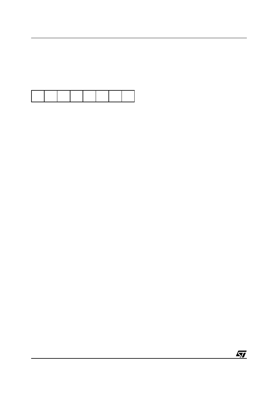
11.4.7 Register Description
I2C CONTROL REGISTER (CR)
Read / Write
Reset Value: 0000 0000 (00h)
Bit 7:6 = Reserved. Forced to 0 by hardware.
Bit 5 = PE Peripheral enable.
This bit is set and cleared by software.
0: Peripheral disabled
1: Master/Slave capability
Notes:
– When PE=0, all the bits of the CR register and
the SR register except the Stop bit are reset. All
outputs are released while PE=0
– When PE=1, the corresponding I/O pins are se-
lected by hardware as alternate functions.
– To enable the I2C interface, write the CR register
TWICE with PE=1 as the first write only activates
the interface (only PE is set).
Bit 4 = ENGC Enable General Call.
This bit is set and cleared by software. It is also
cleared by hardware when the interface is disa-
bled (PE=0). The 00h General Call address is ac-
knowledged (01h ignored).
0: General Call disabled
1: General Call enabled
Bit 3 = START Generation of a Start condition.
This bit is set and cleared by software. It is also
cleared by hardware when the interface is disa-
bled (PE=0) or when the Start condition is sent
(with interrupt generation if ITE=1).
– In master mode:
0: No start generation
1: Repeated start generation
– In slave mode:
0: No start generation
1: Start generation when the bus is free
Bit 2 = ACK Acknowledge enable.
This bit is set and cleared by software. It is also
cleared by hardware when the interface is disa-
bled (PE=0).
0: No acknowledge returned
1: Acknowledge returned after an address byte or
a data byte is received
Bit 1 = STOP Generation of a Stop condition.
This bit is set and cleared by software. It is also
cleared by hardware in master mode. Note: This
bit is not cleared when the interface is disabled
(PE=0).
– In master mode:
0: No stop generation
1: Stop generation after the current byte transfer
or after the current Start condition is sent. The
STOP bit is cleared by hardware when the Stop
condition is sent.
– In slave mode:
0: No stop generation
1: Release the SCL and SDA lines after the cur-
rent byte transfer (BTF=1). In this mode the
STOP bit has to be cleared by software.
Bit 0 = ITE Interrupt enable.
This bit is set and cleared by software and cleared
by hardware when the interface is disabled
(PE=0).
0: Interrupts disabled
1: Interrupts enabled
Refer to Figure 4 for the relationship between the
events and the interrupt.
SCL is held low when the ADD10, SB, BTF or
ADSL flags or an EV6 event (See Figure 3) is de-
tected.
70
0
PE
ENGC START
ACK
STOP
ITE
相关PDF资料 |
PDF描述 |
|---|---|
| ST72C254G1M3 | 8-BIT, FLASH, 6 MHz, MICROCONTROLLER, PDSO28 |
| ST72C254G1M6 | 8-BIT, FLASH, 8 MHz, MICROCONTROLLER, PDSO28 |
| ST72C254G2M3 | 8-BIT, FLASH, 6 MHz, MICROCONTROLLER, PDSO28 |
| ST72C254G2M7 | 8-BIT, FLASH, 6 MHz, MICROCONTROLLER, PDSO28 |
| ST72C254G2M1 | 8-BIT, FLASH, 8 MHz, MICROCONTROLLER, PDSO28 |
相关代理商/技术参数 |
参数描述 |
|---|---|
| ST72C216G1M6 | 功能描述:8位微控制器 -MCU Flash 4K SPI/I2C RoHS:否 制造商:Silicon Labs 核心:8051 处理器系列:C8051F39x 数据总线宽度:8 bit 最大时钟频率:50 MHz 程序存储器大小:16 KB 数据 RAM 大小:1 KB 片上 ADC:Yes 工作电源电压:1.8 V to 3.6 V 工作温度范围:- 40 C to + 105 C 封装 / 箱体:QFN-20 安装风格:SMD/SMT |
| ST72C254G1B6 | 功能描述:8位微控制器 -MCU Flash 4K SPI/I2C RoHS:否 制造商:Silicon Labs 核心:8051 处理器系列:C8051F39x 数据总线宽度:8 bit 最大时钟频率:50 MHz 程序存储器大小:16 KB 数据 RAM 大小:1 KB 片上 ADC:Yes 工作电源电压:1.8 V to 3.6 V 工作温度范围:- 40 C to + 105 C 封装 / 箱体:QFN-20 安装风格:SMD/SMT |
| ST72C254G1M6 | 功能描述:8位微控制器 -MCU Flash 4K SPI/I2C RoHS:否 制造商:Silicon Labs 核心:8051 处理器系列:C8051F39x 数据总线宽度:8 bit 最大时钟频率:50 MHz 程序存储器大小:16 KB 数据 RAM 大小:1 KB 片上 ADC:Yes 工作电源电压:1.8 V to 3.6 V 工作温度范围:- 40 C to + 105 C 封装 / 箱体:QFN-20 安装风格:SMD/SMT |
| ST72C254G2B1 | 制造商:STMicroelectronics 功能描述:8-BIT MICROCONTROLLER - Bulk |
| ST72C254G2B6 | 功能描述:8位微控制器 -MCU Flash 8K SPI/I2C RoHS:否 制造商:Silicon Labs 核心:8051 处理器系列:C8051F39x 数据总线宽度:8 bit 最大时钟频率:50 MHz 程序存储器大小:16 KB 数据 RAM 大小:1 KB 片上 ADC:Yes 工作电源电压:1.8 V to 3.6 V 工作温度范围:- 40 C to + 105 C 封装 / 箱体:QFN-20 安装风格:SMD/SMT |
发布紧急采购,3分钟左右您将得到回复。