- 您现在的位置:买卖IC网 > PDF目录85116 > ST72F324BK6TAE (STMICROELECTRONICS) 8-BIT, FLASH, 8 MHz, MICROCONTROLLER, PQFP32 PDF资料下载
参数资料
| 型号: | ST72F324BK6TAE |
| 厂商: | STMICROELECTRONICS |
| 元件分类: | 微控制器/微处理器 |
| 英文描述: | 8-BIT, FLASH, 8 MHz, MICROCONTROLLER, PQFP32 |
| 封装: | 7 X 7 MM, ROHS COMPLIANT, LQFP-32 |
| 文件页数: | 72/197页 |
| 文件大小: | 3593K |
| 代理商: | ST72F324BK6TAE |
第1页第2页第3页第4页第5页第6页第7页第8页第9页第10页第11页第12页第13页第14页第15页第16页第17页第18页第19页第20页第21页第22页第23页第24页第25页第26页第27页第28页第29页第30页第31页第32页第33页第34页第35页第36页第37页第38页第39页第40页第41页第42页第43页第44页第45页第46页第47页第48页第49页第50页第51页第52页第53页第54页第55页第56页第57页第58页第59页第60页第61页第62页第63页第64页第65页第66页第67页第68页第69页第70页第71页当前第72页第73页第74页第75页第76页第77页第78页第79页第80页第81页第82页第83页第84页第85页第86页第87页第88页第89页第90页第91页第92页第93页第94页第95页第96页第97页第98页第99页第100页第101页第102页第103页第104页第105页第106页第107页第108页第109页第110页第111页第112页第113页第114页第115页第116页第117页第118页第119页第120页第121页第122页第123页第124页第125页第126页第127页第128页第129页第130页第131页第132页第133页第134页第135页第136页第137页第138页第139页第140页第141页第142页第143页第144页第145页第146页第147页第148页第149页第150页第151页第152页第153页第154页第155页第156页第157页第158页第159页第160页第161页第162页第163页第164页第165页第166页第167页第168页第169页第170页第171页第172页第173页第174页第175页第176页第177页第178页第179页第180页第181页第182页第183页第184页第185页第186页第187页第188页第189页第190页第191页第192页第193页第194页第195页第196页第197页
Obsolete
- Obsolete
Product(s)
ST72324B-Auto
Electrical characteristics
163/197
12.9
I/O port pin characteristics
12.9.1
General characteristics
Subject to general operating conditions for VDD, fOSC, and TA unless otherwise specified.
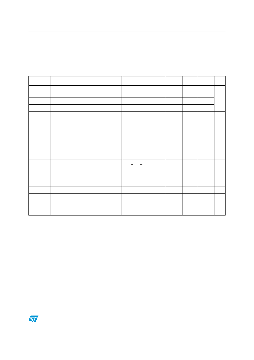
Table 105.
General characteristics
Symbol
Parameter
Conditions
Min
Typ
Max
Unit
VIL
Input low level voltage
(standard voltage devices)(1)
0.3xVDD
V
VIH
Input high level voltage(1)
0.7xVDD
Vhys
Schmitt trigger voltage hysteresis(2)
0.7
IINJ(PIN)
(3)
Injected current on I/O pins other than
pin PB0(4)
VDD = 5V
±4
mA
Injected current on ROM and 32 Kbyte
Flash devices pin PB0
Injected current on 8/16 Kbyte Flash
devices pin PB0
0+4
ΣI
INJ(PIN)
(3) Total injected current
(sum of all I/O and control pins)
VDD = 5V
±25
mA
Ilkg
Input leakage current
VSS < VIN < VDD
±1
A
IS
Static current consumption induced by
each floating input pin
Floating input mode(5)(6)
200
RPU
Weak pull-up equivalent resistor(7)
VIN = VSS, VDD = 5V
50
120
250
k
CIO
I/O pin capacitance
5
pF
tf(IO)out
Output high to low level fall time(1)
CL = 50pF
between 10% and 90%
25
ns
tr(IO)out
Output low to high level rise time(1)
25
tw(IT)in
External interrupt pulse time(8)
1tCPU
1.
Data based on characterization results, not tested in production.
2.
Hysteresis voltage between Schmitt trigger switching levels. Based on characterization results, not tested.
3.
When the current limitation is not possible, the VIN maximum must be respected, otherwise refer to the IINJ(PIN)
specification. A positive injection is induced by VIN >VDD while a negative injection is induced by VIN <VSS. Refer to
Section 12.2.2 on page 149 for more details.
4.
No negative current injection allowed on 8/16 Kbyte Flash devices
5.
Static peak current value taken at a fixed VIN value, based on design simulation and technology characteristics, not tested
in production. This value depends on VDD and temperature values.
6.
The Schmitt trigger that is connected to every I/O port is disabled for analog inputs only when ADON bit is ON and the
particular ADC channel is selected (with port configured in input floating mode). When the ADON bit is OFF, static current
consumption may result. This can be avoided by keeping the input voltage of this pin close to VDD or VSS.
7.
The RPU pull-up equivalent resistor is based on a resistive transistor (corresponding IPU current characteristics described in
8.
To generate an external interrupt, a minimum pulse width has to be applied on an I/O port pin configured as an external
interrupt source.
相关PDF资料 |
PDF描述 |
|---|---|
| ST72321B(AR9)TA/XXXE | 8-BIT, MROM, 16 MHz, MICROCONTROLLER, PQFP64 |
| ST72321B(R6)TB/XXXRE | 8-BIT, MROM, 16 MHz, MICROCONTROLLER, PQFP64 |
| ST72F321BJ7TAE | 8-BIT, FLASH, 8 MHz, MICROCONTROLLER, PQFP44 |
| ST72P321B(AR7)TCXXXRE | 8-BIT, MROM, 16 MHz, MICROCONTROLLER, PQFP64 |
| S3S12P128J0CLH | 16-BIT, MROM, 1.05 MHz, MICROCONTROLLER, PQFP64 |
相关代理商/技术参数 |
参数描述 |
|---|---|
| ST72F324BK6TAS | 制造商:STMicroelectronics 功能描述:MCU 8BIT ST7 CISC 32KB FLASH 5V 32TQFP - Trays 制造商:STMicroelectronics 功能描述:8-bit MCU for automotive, 3.8 to 5.5V operating range with 8 to 32 Kbyte Flash/ROM, 10-bit ADC, 4 timers, SPI, SCI |
| ST72F324BK6TAXS | 制造商:STMicroelectronics 功能描述: |
| ST72F324BK6TCE | 制造商:STMicroelectronics 功能描述: |
| ST72F324BK6TCS | 制造商:STMicroelectronics 功能描述:APG |
| ST72F324BK6TCTRE | 制造商:STMicroelectronics 功能描述:LQFP 32 7x7x1.4 1 |
发布紧急采购,3分钟左右您将得到回复。