- 您现在的位置:买卖IC网 > PDF目录98145 > ST72F324K4B6 (STMICROELECTRONICS) 8-BIT, FLASH, 8 MHz, MICROCONTROLLER, PDIP32 PDF资料下载
参数资料
| 型号: | ST72F324K4B6 |
| 厂商: | STMICROELECTRONICS |
| 元件分类: | 微控制器/微处理器 |
| 英文描述: | 8-BIT, FLASH, 8 MHz, MICROCONTROLLER, PDIP32 |
| 封装: | 0.400 INCH, PLASTIC, SDIP-32 |
| 文件页数: | 43/156页 |
| 文件大小: | 1027K |
| 代理商: | ST72F324K4B6 |
第1页第2页第3页第4页第5页第6页第7页第8页第9页第10页第11页第12页第13页第14页第15页第16页第17页第18页第19页第20页第21页第22页第23页第24页第25页第26页第27页第28页第29页第30页第31页第32页第33页第34页第35页第36页第37页第38页第39页第40页第41页第42页当前第43页第44页第45页第46页第47页第48页第49页第50页第51页第52页第53页第54页第55页第56页第57页第58页第59页第60页第61页第62页第63页第64页第65页第66页第67页第68页第69页第70页第71页第72页第73页第74页第75页第76页第77页第78页第79页第80页第81页第82页第83页第84页第85页第86页第87页第88页第89页第90页第91页第92页第93页第94页第95页第96页第97页第98页第99页第100页第101页第102页第103页第104页第105页第106页第107页第108页第109页第110页第111页第112页第113页第114页第115页第116页第117页第118页第119页第120页第121页第122页第123页第124页第125页第126页第127页第128页第129页第130页第131页第132页第133页第134页第135页第136页第137页第138页第139页第140页第141页第142页第143页第144页第145页第146页第147页第148页第149页第150页第151页第152页第153页第154页第155页第156页
ST72324J/K
137/156
12.9 CONTROL PIN CHARACTERISTICS
12.9.1 Asynchronous RESET Pin
Subject to general operating conditions for VDD,fCPU, and TA unless otherwise specified.
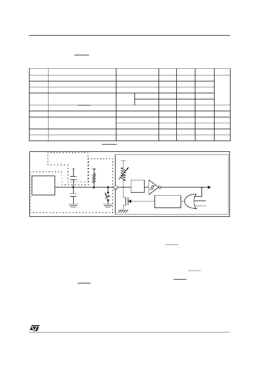
Figure 88. Typical Application with RESET pin
6)7)8)
Notes:
1. Data based on characterization results, not tested in production.
2. Hysteresis voltage between Schmitt trigger switching levels.
3. The IIO current sunk must always respect the absolute maximum rating specified in Section 12.2.2 and the sum of IIO
(I/O ports and control pins) must not exceed IVSS.
4. To guarantee the reset of the device, a minimum pulse has to be applied to the RESET pin. All short pulses applied on
the RESET pin with a duration below th(RSTL)in can be ignored.
5. The reset network (the resistor and two capacitors) protects the device against parasitic resets, especially in noisy en-
vironments.
6. The output of the external reset circuit must have an open-drain output to drive the ST7 reset pad. Otherwise the device
can be damaged when the ST7 generates an internal reset (LVD or watchdog).
7. Whatever the reset source is (internal or external), the user must ensure that the level on the RESET pin can go below
the VIL max. level specified in Section 12.9.1 . Otherwise the reset will not be taken into account internally.
8. Because the reset circuit is designed to allow the internal RESET to be output in the RESET pin, the user must ensure
that the current sunk on the RESET pin (by an external pull-up for example) is less than the absolute maximum value
specified for IINJ(RESET) in Section 12.2.2 on page 113.
9. Data guaranteed by design, not tested in production.
Symbol
Parameter
Condit ions
Min
Typ
Max
Unit
VIL
Input low level voltage 1)
0.16xV
DD
V
VIH
Input high level voltage 1)
0.85xV
DD
Vhys
Schmitt trigger voltage hysteresis 2)
2.5
VOL
Output low level voltage 3)
VDD=5V
IIO=+5mA
0.5
1.2
IIO=+2mA
0.2
0.5
IIO
Input current on RESET pin
2
TBD
mA
RON
Weak pull-up equivalent resistor
20
30
120
k
tw(RSTL)out Generated reset pulse duration
External pin
0
429)
s
Internal reset sources
20
30
429)
s
th(RSTL)in External reset pulse hold time
4)
2.5
s
tg(RSTL)in Filtered glitch duration
5)
200
ns
0.01
F
VDD
0.01
F
EXTERNAL
RESE T
CIRCUIT
5)
USER
VDD
4.7k
Required if LVD is disabled
Recommended
if LVD is disabled
ST72XXX
PULSE
GENERATOR
Filter
RON
VDD
WATCHDOG
LVD RESET
INTERNAL
RESET
相关PDF资料 |
PDF描述 |
|---|---|
| ST72F325C4T6 | 8-BIT, FLASH, 8 MHz, MICROCONTROLLER, PQFP48 |
| ST72325C6T3/XXX | 8-BIT, MROM, 8 MHz, MICROCONTROLLER, PQFP48 |
| ST72F340S2T6 | 8-BIT, FLASH, 8 MHz, MICROCONTROLLER, PQFP44 |
| ST72F340K2T6 | 8-BIT, FLASH, 8 MHz, MICROCONTROLLER, PQFP32 |
| ST72F345N4H6 | 8-BIT, FLASH, 8 MHz, MICROCONTROLLER, PBGA56 |
相关代理商/技术参数 |
参数描述 |
|---|---|
| ST72F324K4T6 | 功能描述:8位微控制器 -MCU Flash 16K SPI/SCI RoHS:否 制造商:Silicon Labs 核心:8051 处理器系列:C8051F39x 数据总线宽度:8 bit 最大时钟频率:50 MHz 程序存储器大小:16 KB 数据 RAM 大小:1 KB 片上 ADC:Yes 工作电源电压:1.8 V to 3.6 V 工作温度范围:- 40 C to + 105 C 封装 / 箱体:QFN-20 安装风格:SMD/SMT |
| ST72F324K4T6TR | 功能描述:8位微控制器 -MCU 5V RANGE 8B MCU RoHS:否 制造商:Silicon Labs 核心:8051 处理器系列:C8051F39x 数据总线宽度:8 bit 最大时钟频率:50 MHz 程序存储器大小:16 KB 数据 RAM 大小:1 KB 片上 ADC:Yes 工作电源电压:1.8 V to 3.6 V 工作温度范围:- 40 C to + 105 C 封装 / 箱体:QFN-20 安装风格:SMD/SMT |
| ST72F324K4TA | 功能描述:8位微控制器 -MCU Flask 16K SPI/SCI RoHS:否 制造商:Silicon Labs 核心:8051 处理器系列:C8051F39x 数据总线宽度:8 bit 最大时钟频率:50 MHz 程序存储器大小:16 KB 数据 RAM 大小:1 KB 片上 ADC:Yes 工作电源电压:1.8 V to 3.6 V 工作温度范围:- 40 C to + 105 C 封装 / 箱体:QFN-20 安装风格:SMD/SMT |
| ST72F324K4TA/TR | 功能描述:8位微控制器 -MCU AUTO 8BIT MICRO RoHS:否 制造商:Silicon Labs 核心:8051 处理器系列:C8051F39x 数据总线宽度:8 bit 最大时钟频率:50 MHz 程序存储器大小:16 KB 数据 RAM 大小:1 KB 片上 ADC:Yes 工作电源电压:1.8 V to 3.6 V 工作温度范围:- 40 C to + 105 C 封装 / 箱体:QFN-20 安装风格:SMD/SMT |
| ST72F324K4TAE | 功能描述:8位微控制器 -MCU 5V RANGE 8B MCU RoHS:否 制造商:Silicon Labs 核心:8051 处理器系列:C8051F39x 数据总线宽度:8 bit 最大时钟频率:50 MHz 程序存储器大小:16 KB 数据 RAM 大小:1 KB 片上 ADC:Yes 工作电源电压:1.8 V to 3.6 V 工作温度范围:- 40 C to + 105 C 封装 / 箱体:QFN-20 安装风格:SMD/SMT |
发布紧急采购,3分钟左右您将得到回复。