- 您现在的位置:买卖IC网 > PDF目录69362 > ST72F561AR6T6 (STMICROELECTRONICS) 8-BIT, FLASH, 8 MHz, MICROCONTROLLER, PQFP64 PDF资料下载
参数资料
| 型号: | ST72F561AR6T6 |
| 厂商: | STMICROELECTRONICS |
| 元件分类: | 微控制器/微处理器 |
| 英文描述: | 8-BIT, FLASH, 8 MHz, MICROCONTROLLER, PQFP64 |
| 封装: | 10 X 10 MM, LQFP-64 |
| 文件页数: | 54/265页 |
| 文件大小: | 9379K |
| 代理商: | ST72F561AR6T6 |
第1页第2页第3页第4页第5页第6页第7页第8页第9页第10页第11页第12页第13页第14页第15页第16页第17页第18页第19页第20页第21页第22页第23页第24页第25页第26页第27页第28页第29页第30页第31页第32页第33页第34页第35页第36页第37页第38页第39页第40页第41页第42页第43页第44页第45页第46页第47页第48页第49页第50页第51页第52页第53页当前第54页第55页第56页第57页第58页第59页第60页第61页第62页第63页第64页第65页第66页第67页第68页第69页第70页第71页第72页第73页第74页第75页第76页第77页第78页第79页第80页第81页第82页第83页第84页第85页第86页第87页第88页第89页第90页第91页第92页第93页第94页第95页第96页第97页第98页第99页第100页第101页第102页第103页第104页第105页第106页第107页第108页第109页第110页第111页第112页第113页第114页第115页第116页第117页第118页第119页第120页第121页第122页第123页第124页第125页第126页第127页第128页第129页第130页第131页第132页第133页第134页第135页第136页第137页第138页第139页第140页第141页第142页第143页第144页第145页第146页第147页第148页第149页第150页第151页第152页第153页第154页第155页第156页第157页第158页第159页第160页第161页第162页第163页第164页第165页第166页第167页第168页第169页第170页第171页第172页第173页第174页第175页第176页第177页第178页第179页第180页第181页第182页第183页第184页第185页第186页第187页第188页第189页第190页第191页第192页第193页第194页第195页第196页第197页第198页第199页第200页第201页第202页第203页第204页第205页第206页第207页第208页第209页第210页第211页第212页第213页第214页第215页第216页第217页第218页第219页第220页第221页第222页第223页第224页第225页第226页第227页第228页第229页第230页第231页第232页第233页第234页第235页第236页第237页第238页第239页第240页第241页第242页第243页第244页第245页第246页第247页第248页第249页第250页第251页第252页第253页第254页第255页第256页第257页第258页第259页第260页第261页第262页第263页第264页第265页
ST72561
147/265
LINSCI
SERIAL COMMUNICATION INTERFACE (LIN Mode) (cont’d)
10.7.10 LIN Mode Register Description
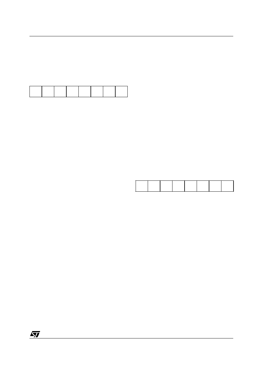
STATUS REGISTER (SCISR)
Read Only
Reset Value: 1100 0000 (C0h)
Bits 7:4 = Same function as in SCI mode; please
refer to Section 0.1.8 SCI Mode Register Descrip-
tion.
Bit 3 = LHE LIN Header Error.
During LIN Header this bit signals three error
types:
– The LIN Synch Field is corrupted and the SCI is
blocked in LIN Synch State (LSF bit = 1).
– A timeout occurred during LIN Header reception
– An overrun error was detected on one of the
header field (see OR bit description in Section
0.1.8 SCI Mode Register Description).
An interrupt is generated if RIE = 1 in the SCICR2
register. If blocked in the LIN Synch State, the LSF
bit must first be reset (to exit LIN Synch Field state
and then to be able to clear LHE flag). Then it is
cleared by the following software sequence: An
access to the SCISR register followed by a read to
the SCIDR register.
0: No LIN Header error
1: LIN Header error detected
Note:
Apart from the LIN Header this bit signals an Over-
run Error as in SCI mode (see description in Sec-
tion 0.1.8 SCI Mode Register Description).
Bit 2 = NF Noise flag
In LIN Master mode (LINE bit = 1 and LSLV bit =
0), this bit has the same function as in SCI mode;
please refer to Section 0.1.8 SCI Mode Register
Description.
In LIN Slave mode (LINE bit = 1 and LSLV bit = 1)
this bit has no meaning.
Bit 1 = FE Framing error.
In LIN slave mode, this bit is set only when a real
framing error is detected (if the stop bit is dominant
(0) and at least one of the other bits is recessive
(1). It is not set when a break occurs, the LHDF bit
is used instead as a break flag (if the LHDM
bit = 0). It is cleared by a software sequence (an
access to the SCISR register followed by a read to
the SCIDR register).
0: No Framing error
1: Framing error detected
Bit 0 = PE Parity error.
This bit is set by hardware when a LIN parity error
occurs (if the PCE bit is set) in receiver mode. It is
cleared by a software sequence (a read to the sta-
tus register followed by an access to the SCIDR
data register). An interrupt is generated if PIE = 1
in the SCICR1 register.
0: No LIN parity error
1: LIN Parity error detected
CONTROL REGISTER 1 (SCICR1)
Read/Write
Reset Value: x000 0000 (x0h)
Bits 7:3 = Same function as in SCI mode; please
refer to Section 0.1.8 SCI Mode Register Descrip-
tion.
Bit 2 = PCE Parity control enable.
This bit is set and cleared by software. It selects
the hardware parity control for LIN identifier parity
check.
0: Parity control disabled
1: Parity control enabled
When a parity error occurs, the PE bit in the
SCISR register is set.
Bit 1 = Reserved
Bit 0 = Same function as in SCI mode; please refer
to Section 0.1.8 SCI Mode Register Description.
7
0
TDRE
TC
RDRF
IDLE
LHE
NF
FE
PE
7
0
R8
T8
SCID
M
WAKE
PCE
PS
PIE
相关PDF资料 |
PDF描述 |
|---|---|
| ST72F561AR7T6 | 8-BIT, FLASH, 8 MHz, MICROCONTROLLER, PQFP64 |
| ST72F561AR9T6 | 8-BIT, FLASH, 8 MHz, MICROCONTROLLER, PQFP64 |
| ST72F561K7T6 | 8-BIT, FLASH, 8 MHz, MICROCONTROLLER, PQFP32 |
| ST72F561K9T6 | 8-BIT, FLASH, 8 MHz, MICROCONTROLLER, PQFP32 |
| ST72P561K7T3/XXX | 8-BIT, MROM, 8 MHz, MICROCONTROLLER, PQFP32 |
相关代理商/技术参数 |
参数描述 |
|---|---|
| ST72F561AR6TAE | 功能描述:8位微控制器 -MCU 8B MCU RoHS:否 制造商:Silicon Labs 核心:8051 处理器系列:C8051F39x 数据总线宽度:8 bit 最大时钟频率:50 MHz 程序存储器大小:16 KB 数据 RAM 大小:1 KB 片上 ADC:Yes 工作电源电压:1.8 V to 3.6 V 工作温度范围:- 40 C to + 105 C 封装 / 箱体:QFN-20 安装风格:SMD/SMT |
| ST72F561AR6TCE | 制造商:STMicroelectronics 功能描述: |
| ST72F561AR7T6 | 功能描述:8位微控制器 -MCU ST72561 8B MCU RoHS:否 制造商:Silicon Labs 核心:8051 处理器系列:C8051F39x 数据总线宽度:8 bit 最大时钟频率:50 MHz 程序存储器大小:16 KB 数据 RAM 大小:1 KB 片上 ADC:Yes 工作电源电压:1.8 V to 3.6 V 工作温度范围:- 40 C to + 105 C 封装 / 箱体:QFN-20 安装风格:SMD/SMT |
| ST72F561AR7TAE | 功能描述:8位微控制器 -MCU 8B MCU RoHS:否 制造商:Silicon Labs 核心:8051 处理器系列:C8051F39x 数据总线宽度:8 bit 最大时钟频率:50 MHz 程序存储器大小:16 KB 数据 RAM 大小:1 KB 片上 ADC:Yes 工作电源电压:1.8 V to 3.6 V 工作温度范围:- 40 C to + 105 C 封装 / 箱体:QFN-20 安装风格:SMD/SMT |
| ST72F561AR7TATRE | 制造商:STMicroelectronics 功能描述: |
发布紧急采购,3分钟左右您将得到回复。