- 您现在的位置:买卖IC网 > PDF目录69369 > ST72F621J4B1 (STMICROELECTRONICS) 8-BIT, FLASH, 8 MHz, MICROCONTROLLER, PDIP42 PDF资料下载
参数资料
| 型号: | ST72F621J4B1 |
| 厂商: | STMICROELECTRONICS |
| 元件分类: | 微控制器/微处理器 |
| 英文描述: | 8-BIT, FLASH, 8 MHz, MICROCONTROLLER, PDIP42 |
| 封装: | 0.600 INCH, LEAD FREE, SHRINK, PLASTIC, DIP-42 |
| 文件页数: | 101/139页 |
| 文件大小: | 1264K |
| 代理商: | ST72F621J4B1 |
第1页第2页第3页第4页第5页第6页第7页第8页第9页第10页第11页第12页第13页第14页第15页第16页第17页第18页第19页第20页第21页第22页第23页第24页第25页第26页第27页第28页第29页第30页第31页第32页第33页第34页第35页第36页第37页第38页第39页第40页第41页第42页第43页第44页第45页第46页第47页第48页第49页第50页第51页第52页第53页第54页第55页第56页第57页第58页第59页第60页第61页第62页第63页第64页第65页第66页第67页第68页第69页第70页第71页第72页第73页第74页第75页第76页第77页第78页第79页第80页第81页第82页第83页第84页第85页第86页第87页第88页第89页第90页第91页第92页第93页第94页第95页第96页第97页第98页第99页第100页当前第101页第102页第103页第104页第105页第106页第107页第108页第109页第110页第111页第112页第113页第114页第115页第116页第117页第118页第119页第120页第121页第122页第123页第124页第125页第126页第127页第128页第129页第130页第131页第132页第133页第134页第135页第136页第137页第138页第139页
ST7262xxx
64/139
Doc ID 6996 Rev 5
SERIAL PERIPHERAL INTERFACE (Cont’d)
10.4.8 Register Description
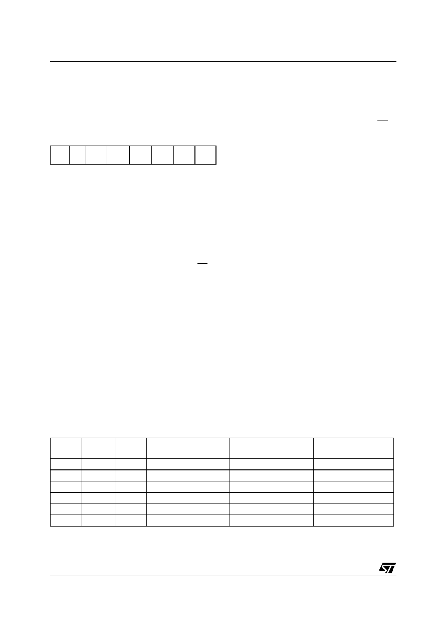
CONTROL REGISTER (SPICR)
Read/Write
Reset Value: 0000 xxxx (0xh)
Bit 7 = SPIE Serial Peripheral Interrupt Enable.
This bit is set and cleared by software.
0: Interrupt is inhibited
1: An SPI interrupt is generated whenever
SPIF=1, MODF=1 or OVR=1 in the SPICSR
register
Bit 6 = SPE Serial Peripheral Output Enable.
This bit is set and cleared by software. It is also
cleared by hardware when, in master mode, SS=0
(see
(MODF)). The SPE bit is cleared by reset, so the
SPI peripheral is not initially connected to the ex-
ternal pins.
0: I/O pins free for general purpose I/O
1: SPI I/O pin alternate functions enabled
Bit 5 = SPR2 Divider Enable.
This bit is set and cleared by software and is
cleared by reset. It is used with the SPR[1:0] bits to
set the baud rate. Refer to Table 18 SPI Master
0: Divider by 2 enabled
1: Divider by 2 disabled
Note: This bit has no effect in slave mode.
Bit 4 = MSTR Master Mode.
This bit is set and cleared by software. It is also
cleared by hardware when, in master mode, SS=0
(see
(MODF)).
0: Slave mode
1: Master mode. The function of the SCK pin
changes from an input to an output and the func-
tions of the MISO and MOSI pins are reversed.
Bit 3 = CPOL Clock Polarity.
This bit is set and cleared by software. This bit de-
termines the idle state of the serial Clock. The
CPOL bit affects both the master and slave
modes.
0: SCK pin has a low level idle state
1: SCK pin has a high level idle state
Note: If CPOL is changed at the communication
byte boundaries, the SPI must be disabled by re-
setting the SPE bit.
Bit 2 = CPHA Clock Phase.
This bit is set and cleared by software.
0: The first clock transition is the first data capture
edge.
1: The second clock transition is the first capture
edge.
Note: The slave must have the same CPOL and
CPHA settings as the master.
Bits 1:0 = SPR[1:0] Serial Clock Frequency.
These bits are set and cleared by software. Used
with the SPR2 bit, they select the baud rate of the
SPI serial clock SCK output by the SPI in master
mode.
Note: These 2 bits have no effect in slave mode.
Table 18. SPI Master mode SCK Frequency
70
SPIE
SPE
SPR2
MSTR
CPOL
CPHA
SPR1
SPR0
SPR2
SPR1
SPR0
Serial Clock
(fCPU = 8MHz)
Serial Clock
(fCPU= 4MHz)
SCK
10
0
fCPU/4
fCPU/2
2 MHz
00
0
fCPU/8
fCPU/4
1 MHz
00
1
fCPU/16
fCPU/8
0.5 MHz
11
0
fCPU/32
fCPU/16
0.25 MHz
01
0
fCPU/64
fCPU/32
125 kHz
01
1
fCPU/128
fCPU/64
62.5 kHz
相关PDF资料 |
PDF描述 |
|---|---|
| ST72621K4B1 | 8-BIT, FLASH, 8 MHz, MICROCONTROLLER, PDIP32 |
| ST72P324BJ6TA/XXXRE | 8-BIT, MROM, 8 MHz, MICROCONTROLLER, PQFP44 |
| ST72P324BK6TA/XXXRE | 8-BIT, MROM, 8 MHz, MICROCONTROLLER, PQFP32 |
| ST72F324BK2TCRS | 8-BIT, FLASH, 8 MHz, MICROCONTROLLER, PQFP32 |
| ST72F324BK4TCRS | 8-BIT, FLASH, 8 MHz, MICROCONTROLLER, PQFP32 |
相关代理商/技术参数 |
参数描述 |
|---|---|
| ST72F621J4D0 | 功能描述:8位微控制器 -MCU Flash 16K USB/SPI/SC RoHS:否 制造商:Silicon Labs 核心:8051 处理器系列:C8051F39x 数据总线宽度:8 bit 最大时钟频率:50 MHz 程序存储器大小:16 KB 数据 RAM 大小:1 KB 片上 ADC:Yes 工作电源电压:1.8 V to 3.6 V 工作温度范围:- 40 C to + 105 C 封装 / 箱体:QFN-20 安装风格:SMD/SMT |
| ST72F621J4T1 | 功能描述:8位微控制器 -MCU ST7262 Lo Spd USB 8B MCU RoHS:否 制造商:Silicon Labs 核心:8051 处理器系列:C8051F39x 数据总线宽度:8 bit 最大时钟频率:50 MHz 程序存储器大小:16 KB 数据 RAM 大小:1 KB 片上 ADC:Yes 工作电源电压:1.8 V to 3.6 V 工作温度范围:- 40 C to + 105 C 封装 / 箱体:QFN-20 安装风格:SMD/SMT |
| ST72F621K4B1 | 功能描述:8位微控制器 -MCU Flash 16K USB/SPI/SC RoHS:否 制造商:Silicon Labs 核心:8051 处理器系列:C8051F39x 数据总线宽度:8 bit 最大时钟频率:50 MHz 程序存储器大小:16 KB 数据 RAM 大小:1 KB 片上 ADC:Yes 工作电源电压:1.8 V to 3.6 V 工作温度范围:- 40 C to + 105 C 封装 / 箱体:QFN-20 安装风格:SMD/SMT |
| ST72F621L4M1 | 功能描述:8位微控制器 -MCU Flash 16K USB/SPI/SC RoHS:否 制造商:Silicon Labs 核心:8051 处理器系列:C8051F39x 数据总线宽度:8 bit 最大时钟频率:50 MHz 程序存储器大小:16 KB 数据 RAM 大小:1 KB 片上 ADC:Yes 工作电源电压:1.8 V to 3.6 V 工作温度范围:- 40 C to + 105 C 封装 / 箱体:QFN-20 安装风格:SMD/SMT |
| ST72F621L4M1 | 制造商:STMicroelectronics 功能描述:8-BIT MICROCONTROLLER IC |
发布紧急采购,3分钟左右您将得到回复。