- 您现在的位置:买卖IC网 > PDF目录25648 > ST72P321B(AR6)TCXXXE (STMICROELECTRONICS) 8-BIT, MROM, 16 MHz, MICROCONTROLLER, PQFP64 PDF资料下载
参数资料
| 型号: | ST72P321B(AR6)TCXXXE |
| 厂商: | STMICROELECTRONICS |
| 元件分类: | 微控制器/微处理器 |
| 英文描述: | 8-BIT, MROM, 16 MHz, MICROCONTROLLER, PQFP64 |
| 封装: | 10 X 10 MM, LQFP-64 |
| 文件页数: | 108/247页 |
| 文件大小: | 4195K |
| 代理商: | ST72P321B(AR6)TCXXXE |
第1页第2页第3页第4页第5页第6页第7页第8页第9页第10页第11页第12页第13页第14页第15页第16页第17页第18页第19页第20页第21页第22页第23页第24页第25页第26页第27页第28页第29页第30页第31页第32页第33页第34页第35页第36页第37页第38页第39页第40页第41页第42页第43页第44页第45页第46页第47页第48页第49页第50页第51页第52页第53页第54页第55页第56页第57页第58页第59页第60页第61页第62页第63页第64页第65页第66页第67页第68页第69页第70页第71页第72页第73页第74页第75页第76页第77页第78页第79页第80页第81页第82页第83页第84页第85页第86页第87页第88页第89页第90页第91页第92页第93页第94页第95页第96页第97页第98页第99页第100页第101页第102页第103页第104页第105页第106页第107页当前第108页第109页第110页第111页第112页第113页第114页第115页第116页第117页第118页第119页第120页第121页第122页第123页第124页第125页第126页第127页第128页第129页第130页第131页第132页第133页第134页第135页第136页第137页第138页第139页第140页第141页第142页第143页第144页第145页第146页第147页第148页第149页第150页第151页第152页第153页第154页第155页第156页第157页第158页第159页第160页第161页第162页第163页第164页第165页第166页第167页第168页第169页第170页第171页第172页第173页第174页第175页第176页第177页第178页第179页第180页第181页第182页第183页第184页第185页第186页第187页第188页第189页第190页第191页第192页第193页第194页第195页第196页第197页第198页第199页第200页第201页第202页第203页第204页第205页第206页第207页第208页第209页第210页第211页第212页第213页第214页第215页第216页第217页第218页第219页第220页第221页第222页第223页第224页第225页第226页第227页第228页第229页第230页第231页第232页第233页第234页第235页第236页第237页第238页第239页第240页第241页第242页第243页第244页第245页第246页第247页
Electrical characteristics
ST72321Bxxx-Auto
196/223
19.4
Supply current characteristics
The following current consumption specified for the ST7 functional operating modes over
temperature range does not take into account the clock source current consumption. To
obtain the total device consumption, the two current values must be added (except for Halt
mode, for which the clock is stopped).
19.4.1
Current consumption
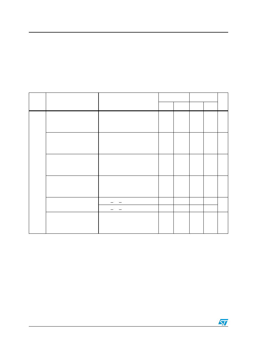
Table 110.
Current consumption
Symbol
Parameter
Conditions
Flash devices
ROM devices
Unit
Typ
Max(1)
Typ
Max(1)
IDD
Supply current in Run
mode(2)
fOSC = 2 MHz, fCPU =1MHz
fOSC = 4 MHz, fCPU =2MHz
fOSC = 8 MHz, fCPU =4MHz
fOSC =16MHz, fCPU =8MHz
1.3
2.0
3.6
7.1
3.0
5.0
8.0
15.0
0.5
1.2
2.2
4.8
1.0
2.0
4.0
8.0
mA
Supply current in Slow
mode(2)
fOSC = 2 MHz, fCPU = 62.5 kHz
fOSC = 4 MHz, fCPU = 125 kHz
fOSC = 8 MHz, fCPU = 250 kHz
fOSC =16MHz, fCPU =500 kHz
600
700
800
1100
2700
3000
3600
4000
100
200
300
500
600
700
800
950
A
Supply current in Wait
mode(2)
fOSC = 2 MHz, fCPU =1MHz
fOSC = 4 MHz, fCPU =2MHz
fOSC = 8 MHz, fCPU =4MHz
fOSC =16MHz, fCPU =8MHz
0.8
1.2
2.0
3.5
3.0
4.0
5.0
7.0
0.5
0.8
1.5
3.0
1.0
1.3
2.2
4.0
mA
Supply current in Slow Wait
mode(2)
fOSC = 2 MHz, fCPU = 62.5 kHz
fOSC = 4 MHz, fCPU = 125 kHz
fOSC = 8 MHz, fCPU = 250 kHz
fOSC =16MHz, fCPU =500 kHz
580
650
770
1050
1200
1300
1800
2000
50
90
180
350
100
150
300
600
A
Supply current in Halt
mode(3)
-40°C < TA < +85°C
<1
10
<1
10
A
-40°C < TA < +125°C
5
50
<1
50
Supply current in Active Halt
mode(4)
fOSC =2MHz
fOSC =4MHz
fOSC =8MHz
fOSC =16MHz
415
430
460
550
525
550
600
700
15
30
60
120
25
50
100
200
A
1.
Data based on characterization results, tested in production at VDD max. and fCPU max.
2.
Measurements are done in the following conditions:
- Program executed from RAM, CPU running with RAM access
- All I/O pins in input mode with a static value at VDD or VSS (no load)
- All peripherals in reset state
- LVD disabled
- Clock input (OSC1) driven by external square wave
- In Slow and Slow Wait mode, fCPU is based on fOSC divided by 32
- To obtain the total current consumption of the device, add the clock source (Section 19.4.2) and the peripheral power
consumption (Section 19.4.3).
3.
All I/O pins in push-pull 0 mode (when applicable) with a static value at VDD or VSS (no load), LVD disabled. Data based on
characterization results, tested in production at VDD max. and fCPU max.
4.
Data based on characterization results, not tested in production. All I/O pins in push-pull 0 mode (when applicable) with a
static value at VDD or VSS (no load); clock input (OSC1) driven by external square wave, LVD disabled. To obtain the total
current consumption of the device, add the clock source consumption (Section 19.4.2).
相关PDF资料 |
PDF描述 |
|---|---|
| ST72F324BJ2TATRE | 8-BIT, FLASH, 8 MHz, MICROCONTROLLER, PQFP44 |
| ST72F324BK4TCE | 8-BIT, FLASH, 8 MHz, MICROCONTROLLER, PQFP32 |
| ST72P63BH4T1 | 8-BIT, MROM, 8 MHz, MICROCONTROLLER, PQFP48 |
| STF-H240IYD | T-1 DUAL COLOR LED ARRAY, RED/YELLOW, 3 mm |
| STM32F103CBT6 | 32-BIT, FLASH, 72 MHz, RISC MICROCONTROLLER, PQFP48 |
相关代理商/技术参数 |
参数描述 |
|---|---|
| ST72P324TA/OBZTR | 制造商:STMicroelectronics 功能描述: |
| ST72P324TA/OHXTR | 制造商:STMicroelectronics 功能描述: |
| ST72P4T128M-A05AU | 制造商:STEC Inc 功能描述:1GB,ECC,REG,DDR2-400,UNLEAD - Bulk |
| ST72T101G1B6 | 功能描述:8位微控制器 -MCU OTP EPROM 4K SPI RoHS:否 制造商:Silicon Labs 核心:8051 处理器系列:C8051F39x 数据总线宽度:8 bit 最大时钟频率:50 MHz 程序存储器大小:16 KB 数据 RAM 大小:1 KB 片上 ADC:Yes 工作电源电压:1.8 V to 3.6 V 工作温度范围:- 40 C to + 105 C 封装 / 箱体:QFN-20 安装风格:SMD/SMT |
| ST72T101G1M6 | 功能描述:8位微控制器 -MCU OTP EPROM 4K SPI RoHS:否 制造商:Silicon Labs 核心:8051 处理器系列:C8051F39x 数据总线宽度:8 bit 最大时钟频率:50 MHz 程序存储器大小:16 KB 数据 RAM 大小:1 KB 片上 ADC:Yes 工作电源电压:1.8 V to 3.6 V 工作温度范围:- 40 C to + 105 C 封装 / 箱体:QFN-20 安装风格:SMD/SMT |
发布紧急采购,3分钟左右您将得到回复。