- 您现在的位置:买卖IC网 > PDF目录69368 > ST72P561AR9TC/XXX (STMICROELECTRONICS) 8-BIT, MROM, 8 MHz, MICROCONTROLLER, PQFP64 PDF资料下载
参数资料
| 型号: | ST72P561AR9TC/XXX |
| 厂商: | STMICROELECTRONICS |
| 元件分类: | 微控制器/微处理器 |
| 英文描述: | 8-BIT, MROM, 8 MHz, MICROCONTROLLER, PQFP64 |
| 封装: | 10 X 10 MM, ROHS COMPLIANT, LQFP-64 |
| 文件页数: | 5/264页 |
| 文件大小: | 5616K |
| 代理商: | ST72P561AR9TC/XXX |
第1页第2页第3页第4页当前第5页第6页第7页第8页第9页第10页第11页第12页第13页第14页第15页第16页第17页第18页第19页第20页第21页第22页第23页第24页第25页第26页第27页第28页第29页第30页第31页第32页第33页第34页第35页第36页第37页第38页第39页第40页第41页第42页第43页第44页第45页第46页第47页第48页第49页第50页第51页第52页第53页第54页第55页第56页第57页第58页第59页第60页第61页第62页第63页第64页第65页第66页第67页第68页第69页第70页第71页第72页第73页第74页第75页第76页第77页第78页第79页第80页第81页第82页第83页第84页第85页第86页第87页第88页第89页第90页第91页第92页第93页第94页第95页第96页第97页第98页第99页第100页第101页第102页第103页第104页第105页第106页第107页第108页第109页第110页第111页第112页第113页第114页第115页第116页第117页第118页第119页第120页第121页第122页第123页第124页第125页第126页第127页第128页第129页第130页第131页第132页第133页第134页第135页第136页第137页第138页第139页第140页第141页第142页第143页第144页第145页第146页第147页第148页第149页第150页第151页第152页第153页第154页第155页第156页第157页第158页第159页第160页第161页第162页第163页第164页第165页第166页第167页第168页第169页第170页第171页第172页第173页第174页第175页第176页第177页第178页第179页第180页第181页第182页第183页第184页第185页第186页第187页第188页第189页第190页第191页第192页第193页第194页第195页第196页第197页第198页第199页第200页第201页第202页第203页第204页第205页第206页第207页第208页第209页第210页第211页第212页第213页第214页第215页第216页第217页第218页第219页第220页第221页第222页第223页第224页第225页第226页第227页第228页第229页第230页第231页第232页第233页第234页第235页第236页第237页第238页第239页第240页第241页第242页第243页第244页第245页第246页第247页第248页第249页第250页第251页第252页第253页第254页第255页第256页第257页第258页第259页第260页第261页第262页第263页第264页
ST72561-Auto
102/264
8-BIT TIMER (Cont’d)
10.5.3.4 One Pulse Mode
One Pulse mode enables the generation of a
pulse when an external event occurs. This mode is
selected via the OPM bit in the CR2 register.
The one pulse mode uses the Input Capture1
function and the Output Compare1 function.
Procedure:
To use one pulse mode:
1. Load the OC1R register with the value corre-
sponding to the length of the pulse (see the for-
mula in the opposite column).
2. Select the following in the CR1 register:
– Using the OLVL1 bit, select the level to be ap-
plied to the OCMP1 pin after the pulse.
– Using the OLVL2 bit, select the level to be ap-
plied to the OCMP1 pin during the pulse.
– Select the edge of the active transition on the
ICAP1 pin with the IEDG1 bit (the ICAP1 pin
must be configured as floating input).
3. Select the following in the CR2 register:
– Set the OC1E bit, the OCMP1 pin is then ded-
icated to the Output Compare 1 function.
– Set the OPM bit.
– Select the timer clock CC[1:0] (see Table 19
Then, on a valid event on the ICAP1 pin, the coun-
ter is initialized to FCh and OLVL2 bit is loaded on
the OCMP1 pin, the ICF1 bit is set and the value
FFFDh is loaded in the IC1R register.
Because the ICF1 bit is set when an active edge
occurs, an interrupt can be generated if the ICIE
bit is set.
Clearing the Input Capture interrupt request (that
is, clearing the ICFi bit) is done in two steps:
1. Reading the SR register while the ICFi bit is set.
2. An access (read or write) to the ICiLR register.
The OC1R register value required for a specific
timing application can be calculated using the fol-
lowing formula:
Where:
t
= Pulse period (in seconds)
fCPU
= PLL output x2 clock frequency in hertz
(or fOSC/2 if PLL is not enabled)
PRESC = Timer prescaler factor (2, 4, 8 or 8000
depending on the CC[1:0] bits, see Ta-
When the value of the counter is equal to the value
of the contents of the OC1R register, the OLVL1
bit is output on the OCMP1 pin, (See Figure 68).
Notes:
1. The OCF1 bit cannot be set by hardware in one
pulse mode but the OCF2 bit can generate an
Output Compare interrupt.
2. When the Pulse Width Modulation (PWM) and
One Pulse Mode (OPM) bits are both set, the
PWM mode is the only active one.
3. If OLVL1=OLVL2 a continuous signal will be
seen on the OCMP1 pin.
4. The ICAP1 pin can not be used to perform input
capture. The ICAP2 pin can be used to perform
input capture (ICF2 can be set and IC2R can be
loaded) but the user must take care that the
counter is reset each time a valid edge occurs
on the ICAP1 pin and ICF1 can also generates
interrupt if ICIE is set.
5. When one pulse mode is used OC1R is dedi-
cated to this mode. Nevertheless OC2R and
OCF2 can be used to indicate a period of time
has been elapsed but cannot generate an out-
put waveform because the level OLVL2 is dedi-
cated to the one pulse mode.
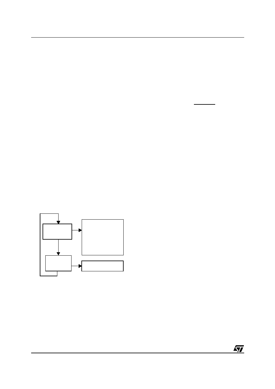
event occurs
Counter
= OC1R
OCMP1 = OLVL1
When
on ICAP1
One pulse mode cycle
OCMP1 = OLVL2
Counter is reset
to FCh
ICF1 bit is set
ICR1 = Counter
OCiR Value =
t * fCPU
PRESC
- 5
相关PDF资料 |
PDF描述 |
|---|---|
| ST72P561K7TA/XXX | 8-BIT, MROM, 8 MHz, MICROCONTROLLER, PQFP32 |
| ST72F561AR4TA | 8-BIT, FLASH, 8 MHz, MICROCONTROLLER, PQFP64 |
| ST72P561AR7TC/XXX | 8-BIT, MROM, 8 MHz, MICROCONTROLLER, PQFP64 |
| ST72561AR6TA/XXX | 8-BIT, MROM, 8 MHz, MICROCONTROLLER, PQFP64 |
| ST72P561AR7TA/XXX | 8-BIT, MROM, 8 MHz, MICROCONTROLLER, PQFP64 |
相关代理商/技术参数 |
参数描述 |
|---|---|
| ST72T101G1B6 | 功能描述:8位微控制器 -MCU OTP EPROM 4K SPI RoHS:否 制造商:Silicon Labs 核心:8051 处理器系列:C8051F39x 数据总线宽度:8 bit 最大时钟频率:50 MHz 程序存储器大小:16 KB 数据 RAM 大小:1 KB 片上 ADC:Yes 工作电源电压:1.8 V to 3.6 V 工作温度范围:- 40 C to + 105 C 封装 / 箱体:QFN-20 安装风格:SMD/SMT |
| ST72T101G1M6 | 功能描述:8位微控制器 -MCU OTP EPROM 4K SPI RoHS:否 制造商:Silicon Labs 核心:8051 处理器系列:C8051F39x 数据总线宽度:8 bit 最大时钟频率:50 MHz 程序存储器大小:16 KB 数据 RAM 大小:1 KB 片上 ADC:Yes 工作电源电压:1.8 V to 3.6 V 工作温度范围:- 40 C to + 105 C 封装 / 箱体:QFN-20 安装风格:SMD/SMT |
| ST72T101G2B6 | 功能描述:8位微控制器 -MCU OTP EPROM 8K SPI RoHS:否 制造商:Silicon Labs 核心:8051 处理器系列:C8051F39x 数据总线宽度:8 bit 最大时钟频率:50 MHz 程序存储器大小:16 KB 数据 RAM 大小:1 KB 片上 ADC:Yes 工作电源电压:1.8 V to 3.6 V 工作温度范围:- 40 C to + 105 C 封装 / 箱体:QFN-20 安装风格:SMD/SMT |
| ST72T101G2M6 | 功能描述:8位微控制器 -MCU RO 511-ST72C104G2M6 RoHS:否 制造商:Silicon Labs 核心:8051 处理器系列:C8051F39x 数据总线宽度:8 bit 最大时钟频率:50 MHz 程序存储器大小:16 KB 数据 RAM 大小:1 KB 片上 ADC:Yes 工作电源电压:1.8 V to 3.6 V 工作温度范围:- 40 C to + 105 C 封装 / 箱体:QFN-20 安装风格:SMD/SMT |
| ST72T121J2B6 | 功能描述:8位微控制器 -MCU OTP EPROM 8K SPI/SCI RoHS:否 制造商:Silicon Labs 核心:8051 处理器系列:C8051F39x 数据总线宽度:8 bit 最大时钟频率:50 MHz 程序存储器大小:16 KB 数据 RAM 大小:1 KB 片上 ADC:Yes 工作电源电压:1.8 V to 3.6 V 工作温度范围:- 40 C to + 105 C 封装 / 箱体:QFN-20 安装风格:SMD/SMT |
发布紧急采购,3分钟左右您将得到回复。