- 您现在的位置:买卖IC网 > PDF目录69373 > ST72T121J2B3 (STMICROELECTRONICS) 8-BIT, OTPROM, 4 MHz, MICROCONTROLLER, PDIP42 PDF资料下载
参数资料
| 型号: | ST72T121J2B3 |
| 厂商: | STMICROELECTRONICS |
| 元件分类: | 微控制器/微处理器 |
| 英文描述: | 8-BIT, OTPROM, 4 MHz, MICROCONTROLLER, PDIP42 |
| 封装: | 0.600 INCH, SHRINK, PLASTIC, DIP-42 |
| 文件页数: | 66/93页 |
| 文件大小: | 597K |
| 代理商: | ST72T121J2B3 |
第1页第2页第3页第4页第5页第6页第7页第8页第9页第10页第11页第12页第13页第14页第15页第16页第17页第18页第19页第20页第21页第22页第23页第24页第25页第26页第27页第28页第29页第30页第31页第32页第33页第34页第35页第36页第37页第38页第39页第40页第41页第42页第43页第44页第45页第46页第47页第48页第49页第50页第51页第52页第53页第54页第55页第56页第57页第58页第59页第60页第61页第62页第63页第64页第65页当前第66页第67页第68页第69页第70页第71页第72页第73页第74页第75页第76页第77页第78页第79页第80页第81页第82页第83页第84页第85页第86页第87页第88页第89页第90页第91页第92页第93页
69/93
ST72E121 ST72T121
SERIAL PERIPHERAL INTERFACE (Cont’d)
5.5.4.4 Write Collision Error
A write collision occurs when the software tries to
write to the DR register while a data transfer is tak-
ing place with an external device. When this hap-
pens, the transfer continues uninterrupted; and
the software write will be unsuccessful.
Write collisions can occur both in master and slave
mode.
Note: a ”read collision” will never occur since the
received data byte is placed in a buffer in which
access is always synchronous with the MCU oper-
ation.
In Slave mode
When the CPHA bit is set:
The slave device will receive a clock (SCK) edge
prior to the latch of the first data transfer. This first
clock edge will freeze the data in the slave device
DR register and output the MSBit on to the exter-
nal MISO pin of the slave device.
The SS pin low state enables the slave device but
the output of the MSBit onto the MISO pin does
not take place until the first data transfer clock
edge.
When the CPHA bit is reset:
Data is latched on the occurrence of the first clock
transition. The slave device does not have any
way of knowing when that transition will occur;
therefore, the slave device collision occurs when
software attempts to write the DR register after its
SS pin has been pulled low.
For this reason, the SS pin must be high, between
each data byte transfer, to allow the CPU to write
in the DR register without generating a write colli-
sion.
In Master mode
Collision in the master device is defined as a write
of the DR register while the internal serial clock
(SCK) is in the process of transfer.
The SS pin signal must be always high on the
master device.
WCOL bit
The WCOL bit in the SR register is set if a write
collision occurs.
No SPI interrupt is generated when the WCOL bit
is set (the WCOL bit is a status flag only).
Clearing the WCOL bit is done through a software
sequence (see Figure 39).
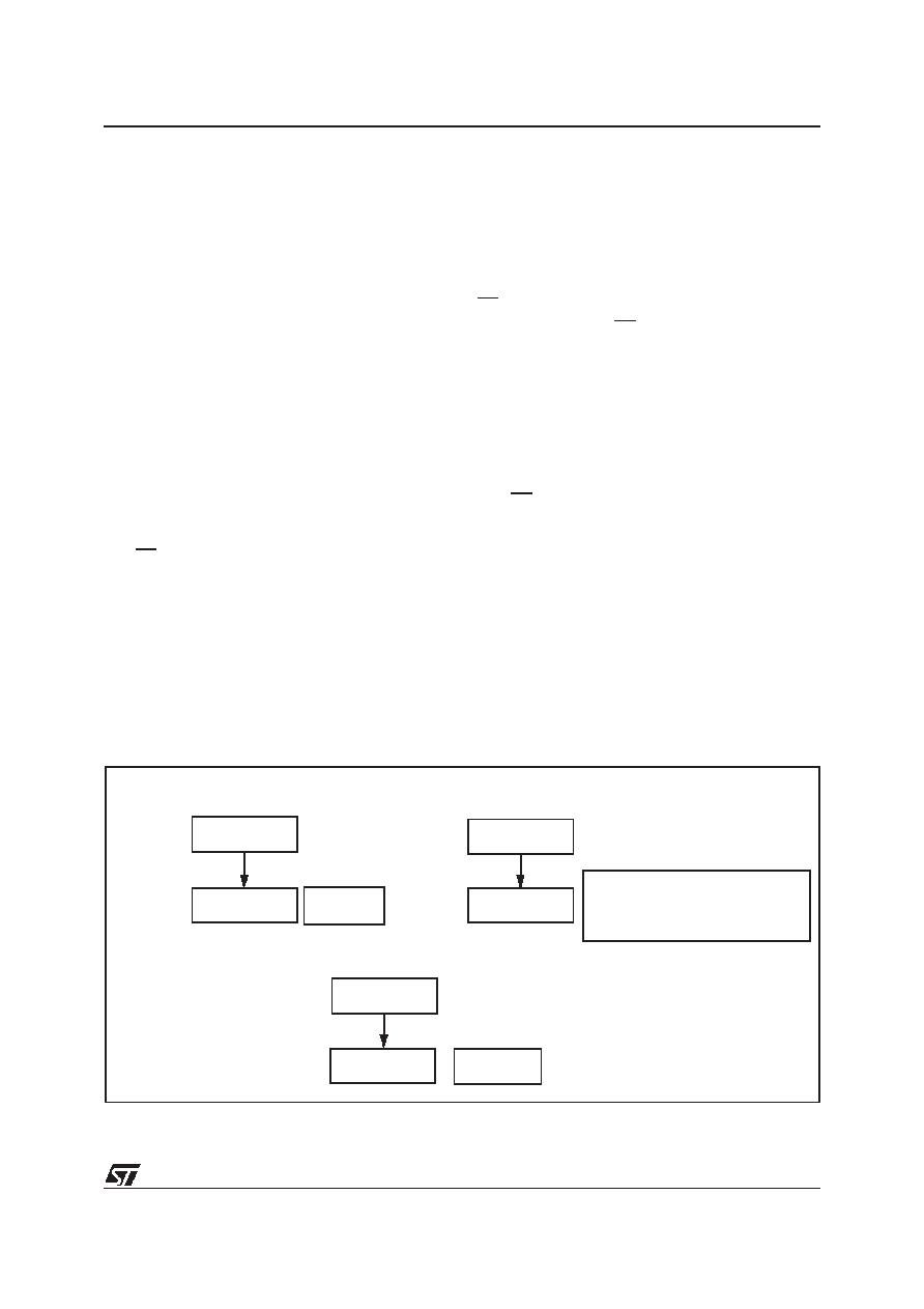
Figure 39. Clearing the WCOL bit (Write Collision Flag) Software Sequence
Clearing sequence after SPIF = 1 (end of a data byte transfer)
1st Step
Read SR
Read DR
Write DR
2nd Step
SPIF =0
WCOL=0
SPIF =0
WCOL=0 if no transfer has started
WCOL=1 if a transfer has started
Clearing sequence before SPIF = 1 (during a data byte transfer)
1st Step
2nd Step
WCOL=0
before the 2nd step
Read SR
Read DR
Note: Writing in DR register in-
stead of reading in it do not reset
WCOL bit
Read SR
OR
THEN
69
相关PDF资料 |
PDF描述 |
|---|---|
| ST72T121J2B6 | 8-BIT, OTPROM, 8 MHz, MICROCONTROLLER, PDIP42 |
| ST72T212G2M6 | 8-BIT, OTPROM, 16 MHz, MICROCONTROLLER, PDSO28 |
| ST72T213G1M3 | 8-BIT, OTPROM, 8 MHz, MICROCONTROLLER, PDSO28 |
| ST72T331N4T1 | 8-BIT, OTPROM, 8 MHz, MICROCONTROLLER, PQFP64 |
| ST72E331J4D0 | 8-BIT, UVPROM, 8 MHz, MICROCONTROLLER, CDIP42 |
相关代理商/技术参数 |
参数描述 |
|---|---|
| ST72T121J2B6 | 功能描述:8位微控制器 -MCU OTP EPROM 8K SPI/SCI RoHS:否 制造商:Silicon Labs 核心:8051 处理器系列:C8051F39x 数据总线宽度:8 bit 最大时钟频率:50 MHz 程序存储器大小:16 KB 数据 RAM 大小:1 KB 片上 ADC:Yes 工作电源电压:1.8 V to 3.6 V 工作温度范围:- 40 C to + 105 C 封装 / 箱体:QFN-20 安装风格:SMD/SMT |
| ST72T121J2T6 | 功能描述:8位微控制器 -MCU OTP EPROM 8K SPI/SCI RoHS:否 制造商:Silicon Labs 核心:8051 处理器系列:C8051F39x 数据总线宽度:8 bit 最大时钟频率:50 MHz 程序存储器大小:16 KB 数据 RAM 大小:1 KB 片上 ADC:Yes 工作电源电压:1.8 V to 3.6 V 工作温度范围:- 40 C to + 105 C 封装 / 箱体:QFN-20 安装风格:SMD/SMT |
| ST72T121J2T6S | 制造商:STMicroelectronics 功能描述: |
| ST72T121J4B6 | 功能描述:8位微控制器 -MCU OTP EPROM 16K SPI/SC RoHS:否 制造商:Silicon Labs 核心:8051 处理器系列:C8051F39x 数据总线宽度:8 bit 最大时钟频率:50 MHz 程序存储器大小:16 KB 数据 RAM 大小:1 KB 片上 ADC:Yes 工作电源电压:1.8 V to 3.6 V 工作温度范围:- 40 C to + 105 C 封装 / 箱体:QFN-20 安装风格:SMD/SMT |
| ST72T121J4T6 | 功能描述:8位微控制器 -MCU OTP EPROM 16K SPI/SC RoHS:否 制造商:Silicon Labs 核心:8051 处理器系列:C8051F39x 数据总线宽度:8 bit 最大时钟频率:50 MHz 程序存储器大小:16 KB 数据 RAM 大小:1 KB 片上 ADC:Yes 工作电源电压:1.8 V to 3.6 V 工作温度范围:- 40 C to + 105 C 封装 / 箱体:QFN-20 安装风格:SMD/SMT |
发布紧急采购,3分钟左右您将得到回复。