- 您现在的位置:买卖IC网 > PDF目录69375 > ST7FL34F2MARS (STMICROELECTRONICS) 8-BIT, FLASH, 8 MHz, MICROCONTROLLER, PDSO20 PDF资料下载
参数资料
| 型号: | ST7FL34F2MARS |
| 厂商: | STMICROELECTRONICS |
| 元件分类: | 微控制器/微处理器 |
| 英文描述: | 8-BIT, FLASH, 8 MHz, MICROCONTROLLER, PDSO20 |
| 封装: | 0.300 INCH, ROHS COMPLIANT, PLASTIC, SOP-20 |
| 文件页数: | 93/236页 |
| 文件大小: | 2064K |
| 代理商: | ST7FL34F2MARS |
第1页第2页第3页第4页第5页第6页第7页第8页第9页第10页第11页第12页第13页第14页第15页第16页第17页第18页第19页第20页第21页第22页第23页第24页第25页第26页第27页第28页第29页第30页第31页第32页第33页第34页第35页第36页第37页第38页第39页第40页第41页第42页第43页第44页第45页第46页第47页第48页第49页第50页第51页第52页第53页第54页第55页第56页第57页第58页第59页第60页第61页第62页第63页第64页第65页第66页第67页第68页第69页第70页第71页第72页第73页第74页第75页第76页第77页第78页第79页第80页第81页第82页第83页第84页第85页第86页第87页第88页第89页第90页第91页第92页当前第93页第94页第95页第96页第97页第98页第99页第100页第101页第102页第103页第104页第105页第106页第107页第108页第109页第110页第111页第112页第113页第114页第115页第116页第117页第118页第119页第120页第121页第122页第123页第124页第125页第126页第127页第128页第129页第130页第131页第132页第133页第134页第135页第136页第137页第138页第139页第140页第141页第142页第143页第144页第145页第146页第147页第148页第149页第150页第151页第152页第153页第154页第155页第156页第157页第158页第159页第160页第161页第162页第163页第164页第165页第166页第167页第168页第169页第170页第171页第172页第173页第174页第175页第176页第177页第178页第179页第180页第181页第182页第183页第184页第185页第186页第187页第188页第189页第190页第191页第192页第193页第194页第195页第196页第197页第198页第199页第200页第201页第202页第203页第204页第205页第206页第207页第208页第209页第210页第211页第212页第213页第214页第215页第216页第217页第218页第219页第220页第221页第222页第223页第224页第225页第226页第227页第228页第229页第230页第231页第232页第233页第234页第235页第236页
Electrical characteristics
ST7L34, ST7L35, ST7L38, ST7L39
182/236
Doc ID 11928 Rev 7
13.2.1
Voltage characteristics
13.2.2
Current characteristics
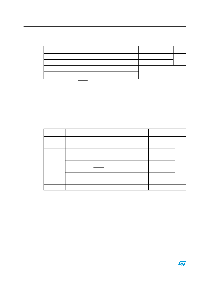
Table 97.
Voltage characteristics
Symbol
Ratings
Maximum value
Unit
VDD - VSS
Supply voltage
7.0
V
VIN
Input voltage on any pin(1)(2)
1.
Directly connecting the RESET and I/O pins to VDD or VSS could damage the device if an unintentional
internal reset is generated or an unexpected change of the I/O configuration occurs (for example, due to a
corrupted program counter). To guarantee safe operation, this connection must be made through a pull-up
or pull-down resistor (typical: 4.7 k
Ω for RESET, 10 kΩ for I/Os). Unused I/O pins must be tied in the same
way to VDD or VSS according to their reset configuration.
2.
IINJ(PIN) must never be exceeded. This is implicitly insured if VIN maximum is respected. If VIN maximum
cannot be respected, the injection current must be limited externally to the IINJ(PIN) value. A positive
injection is induced by VIN >VDD while a negative injection is induced by VIN <VSS. For true open-drain
pads, there is no positive injection current and the corresponding VIN maximum must always be respected
VSS - 0.3 to VDD + 0.3
VESD(HBM)
Electrostatic discharge voltage (human body model)
VESD(MM)
Electrostatic discharge voltage (machine model)
Table 98.
Current characteristics
Symbol
Ratings
Maximum value
Unit
IVDD
Total current into VDD power lines (source)
(1)
1.
All power (VDD) and ground (VSS) lines must always be connected to the external supply.
150
mA
IVSS
150
IIO
Output current sunk by any standard I/O and control pin
20
Output current sunk by any high sink I/O pin
40
Output current source by any I/Os and control pin
- 25
IINJ(PIN)
(2)(3)
2.
IINJ(PIN) must never be exceeded. This is implicitly insured if VIN maximum is respected. If VIN maximum
cannot be respected, the injection current must be limited externally to the IINJ(PIN) value. A positive
injection is induced by VIN >VDD while a negative injection is induced by VIN <VSS.
3.
Negative injection disturbs the analog performance of the device. In particular, it induces leakage currents
throughout the device including the analog inputs. To avoid undesirable effects on the analog functions,
care must be taken:
- Analog input pins must have a negative injection less than 0.8 mA (assuming that the impedance of the
analog voltage is lower than the specified limits)
- Pure digital pins must have a negative injection less than 1.6 mA. In addition, it is recommended to inject
the current as far as possible from the analog input pins.
Injected current on RESET pin
± 5
mA
Injected current on OSC1 and OSC2 pins
± 5
Injected current on any other pin(4)
4.
When several inputs are submitted to a current injection, the maximum
ΣIINJ(PIN) is the absolute sum of the
positive and negative injected currents (instantaneous values). These results are based on
characterization with
ΣIINJ(PIN) maximum current injection on four I/O port pins of the device.
± 5
ΣIINJ(PIN)(2)
Total injected current (sum of all I/O and control pins)(4)
± 20
mA
相关PDF资料 |
PDF描述 |
|---|---|
| ST7FL34F2MAS | 8-BIT, FLASH, 8 MHz, MICROCONTROLLER, PDSO20 |
| ST7FL34F2MCX | 8-BIT, FLASH, 8 MHz, MICROCONTROLLER, PDSO20 |
| ST7FL34F2UAXS | 8-BIT, FLASH, 8 MHz, MICROCONTROLLER, QCC20 |
| ST7FL34F2UCRE | 8-BIT, FLASH, 8 MHz, MICROCONTROLLER, QCC20 |
| ST7FL34F2UCS | 8-BIT, FLASH, 8 MHz, MICROCONTROLLER, QCC20 |
相关代理商/技术参数 |
参数描述 |
|---|---|
| ST7FL34F2MCE | 制造商:STMicroelectronics 功能描述:8-BIT MCU FOR AUTOMOTIVE WITH SINGLE VOLTAGE FLASH/ROM - Rail/Tube |
| ST7FL35F2MAE | 功能描述:8位微控制器 -MCU 8-bit MCU Automotive RoHS:否 制造商:Silicon Labs 核心:8051 处理器系列:C8051F39x 数据总线宽度:8 bit 最大时钟频率:50 MHz 程序存储器大小:16 KB 数据 RAM 大小:1 KB 片上 ADC:Yes 工作电源电压:1.8 V to 3.6 V 工作温度范围:- 40 C to + 105 C 封装 / 箱体:QFN-20 安装风格:SMD/SMT |
| ST7FL35F2MCE | 功能描述:8位微控制器 -MCU 8-BIT MCU AUTOMOTIVE W/SINGLE VOLT FLASH RoHS:否 制造商:Silicon Labs 核心:8051 处理器系列:C8051F39x 数据总线宽度:8 bit 最大时钟频率:50 MHz 程序存储器大小:16 KB 数据 RAM 大小:1 KB 片上 ADC:Yes 工作电源电压:1.8 V to 3.6 V 工作温度范围:- 40 C to + 105 C 封装 / 箱体:QFN-20 安装风格:SMD/SMT |
| ST7FL38F2MAE | 功能描述:8位微控制器 -MCU 8-bit MCU Automotive RoHS:否 制造商:Silicon Labs 核心:8051 处理器系列:C8051F39x 数据总线宽度:8 bit 最大时钟频率:50 MHz 程序存储器大小:16 KB 数据 RAM 大小:1 KB 片上 ADC:Yes 工作电源电压:1.8 V to 3.6 V 工作温度范围:- 40 C to + 105 C 封装 / 箱体:QFN-20 安装风格:SMD/SMT |
| ST7FL38F2MCE | 制造商:STMicroelectronics 功能描述: |
发布紧急采购,3分钟左右您将得到回复。