- 您现在的位置:买卖IC网 > PDF目录69375 > ST7FLIT10BY1B6 (STMICROELECTRONICS) 8-BIT, FLASH, 8 MHz, MICROCONTROLLER, PDIP16 PDF资料下载
参数资料
| 型号: | ST7FLIT10BY1B6 |
| 厂商: | STMICROELECTRONICS |
| 元件分类: | 微控制器/微处理器 |
| 英文描述: | 8-BIT, FLASH, 8 MHz, MICROCONTROLLER, PDIP16 |
| 封装: | 0.300 INCH, ROHS COMPLIANT, PLASTIC, DIP-16 |
| 文件页数: | 5/157页 |
| 文件大小: | 2983K |
| 代理商: | ST7FLIT10BY1B6 |
第1页第2页第3页第4页当前第5页第6页第7页第8页第9页第10页第11页第12页第13页第14页第15页第16页第17页第18页第19页第20页第21页第22页第23页第24页第25页第26页第27页第28页第29页第30页第31页第32页第33页第34页第35页第36页第37页第38页第39页第40页第41页第42页第43页第44页第45页第46页第47页第48页第49页第50页第51页第52页第53页第54页第55页第56页第57页第58页第59页第60页第61页第62页第63页第64页第65页第66页第67页第68页第69页第70页第71页第72页第73页第74页第75页第76页第77页第78页第79页第80页第81页第82页第83页第84页第85页第86页第87页第88页第89页第90页第91页第92页第93页第94页第95页第96页第97页第98页第99页第100页第101页第102页第103页第104页第105页第106页第107页第108页第109页第110页第111页第112页第113页第114页第115页第116页第117页第118页第119页第120页第121页第122页第123页第124页第125页第126页第127页第128页第129页第130页第131页第132页第133页第134页第135页第136页第137页第138页第139页第140页第141页第142页第143页第144页第145页第146页第147页第148页第149页第150页第151页第152页第153页第154页第155页第156页第157页
ST7LITE1xB
102/157
ANALOG COMPARATOR (Cont’d)
11.6.4 Register Description
Internal Voltage Reference Register (VREFCR)
Read/Write
Reset Value : 0000 0000 (00h)
Bit 7 = VCEXT External Voltage Reference for
Comparator
This bit is set or cleared by software. It is used to
connect the external reference voltage to the VN
comparator input.
0: External reference voltage not connected to VN
1: External reference voltage connected to VN
Bit 6 = VCBGR Bandgap Voltage for Comparator
This bit is set or cleared by software. It is used to
connect the bandgap voltage of 1.2V to the VN
comparator input.
0: Bandgap voltage not connected to VN
1: Bandgap voltage connected to VN
Bits 5:2 = VR[3:0] Programmable Internal Voltage
Reference Range Selection
These bits are set or cleared by software. They are
used to select one of 16 different voltages availa-
ble from the internal voltage reference module and
connect it to comparator input VN.
Refer to Table 20.
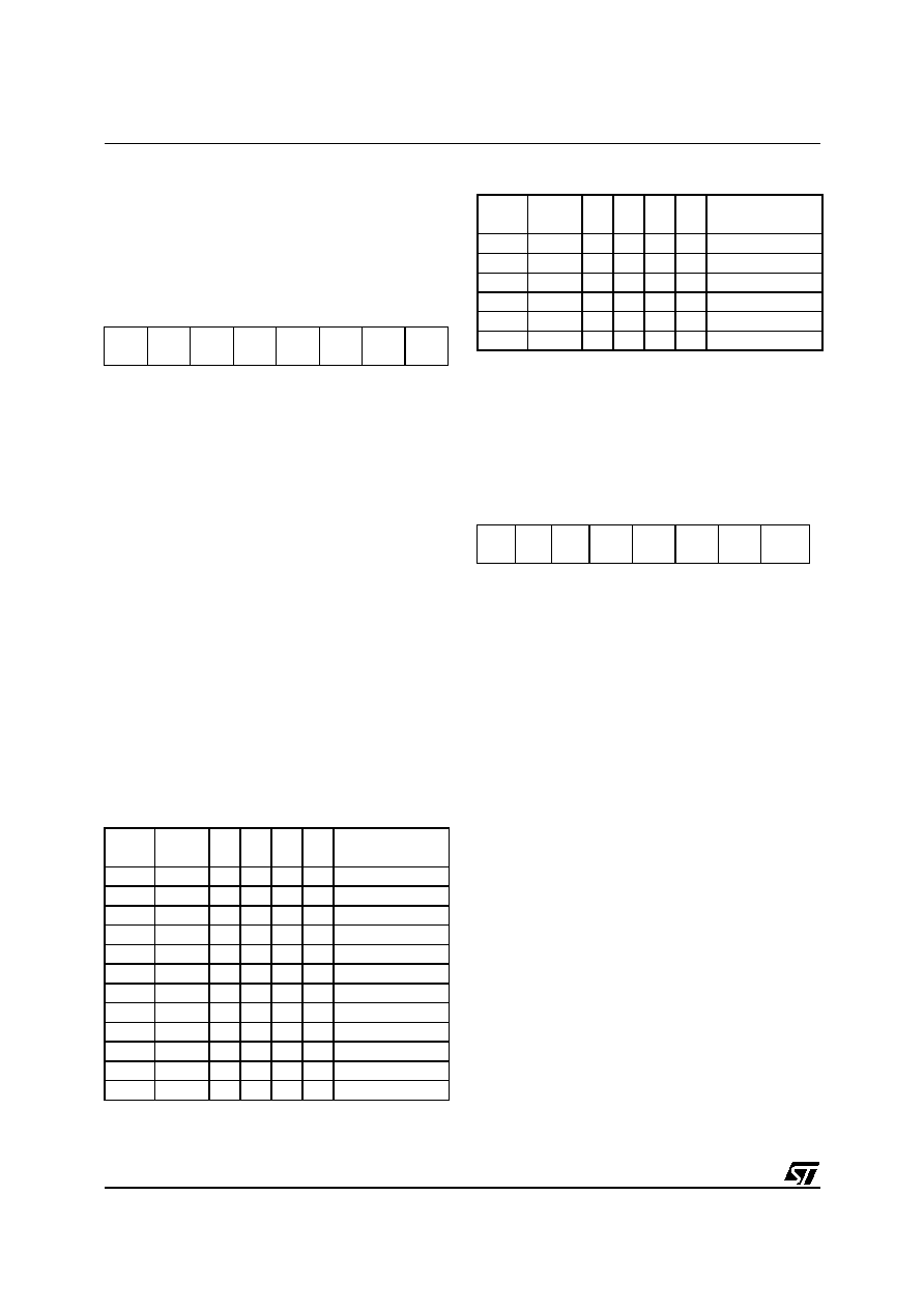
Table 20. Voltage Reference Programming
Bits 1:0 = Reserved, Must be kept cleared.
Comparator Control Register (CMPCR)
Read/Write
Reset Value : 1000 0000 (80h)
Bit 7= CHYST Comparator Hysteresis Enable
This bit is set or cleared by software and set by
hardware reset. When this bit is set, the compara-
tor hysteresis is enabled.
0: Hysteresis disabled
1: Hysteresis enabled
Note: To avoid spurious toggling of the output of
the comparator due to noise on the voltage refer-
ence, it is recommended to enable the hysteresis.
Bit 6 = Reserved, Must be kept cleared
Bit 5 = CINV Comparator Output Inversion Select
This bit is set or cleared by software and cleared
by hardware reset. When this bit is set, the compa-
rator output is inverted.
If interrupt enable bit CMPIE is set in the CMPCR
register, the CINV bit is also used to select which
type of level transition on the comparator output
will generate the interrupt. When this bit is reset,
interrupt will be generated at the rising edge of the
comparator output change (COMP signal, refer to
Figure 62 on page 101). When this bit is set, inter-
rupt will be generated at the falling edge of compa-
rator output change (COMP signal, refer to Figure
0: Comparator output not inverted and interrupt
generated at the rising edge of COMP
1: Comparator output inverted and interrupt gener-
ated at the falling edge of COMP
70
VCEXT VCBGR
VR3
VR2
VR1
VR0
0
VCEXT
bit
VCBGR
bit
VR3
bit
VR2
bit
VR1
bit
VR0
bit
VN Voltage
1
x
VEXT
0
1
x
1.2 bandgap
0
111
1
3.2V
0
111
0
3V
0
110
1
2.8V
0
110
0
2.6V
0
101
1
2.4V
0
101
0
2.2V
0
100
1
2V
0
100
0
1.8V
0
011
1
1.6V
0
011
0
1.4V
0
01
1.2V
0
01
00
1V
0
00
11
0.8V
0
00
10
0.6V
0
00
01
0.4V
0
00
0.2V
70
CHY-
ST
0
CINV CMPIF CMPIE
CMP
COUT CMPON
VCEXT
bit
VCBGR
bit
VR3
bit
VR2
bit
VR1
bit
VR0
bit
VN Voltage
相关PDF资料 |
PDF描述 |
|---|---|
| ST7FLIT15BF1B6 | 8-BIT, FLASH, 8 MHz, MICROCONTROLLER, PDIP20 |
| ST7FLIT19BY0B3 | 8-BIT, FLASH, 8 MHz, MICROCONTROLLER, PDIP16 |
| ST7FLIT19BY1M3 | 8-BIT, FLASH, 8 MHz, MICROCONTROLLER, PDSO16 |
| ST7FLIT10BF0M3 | 8-BIT, FLASH, 8 MHz, MICROCONTROLLER, PDSO20 |
| ST7FLIT10BF0M6 | 8-BIT, FLASH, 8 MHz, MICROCONTROLLER, PDSO20 |
相关代理商/技术参数 |
参数描述 |
|---|---|
| ST7FLIT10BY1BX | 制造商:STMICROELECTRONICS 制造商全称:STMicroelectronics 功能描述:8-BIT MCU WITH SINGLE VOLTAGE FLASH MEMORY, DATA EEPROM, ADC, 5 TIMERS, SPI |
| ST7FLIT10BY1M3 | 制造商:STMicroelectronics 功能描述:ST7FLIT10BY1M3 - Rail/Tube |
| ST7FLIT10BY1M6 | 功能描述:8位微控制器 -MCU ST7LITE1xB 8B MCU RoHS:否 制造商:Silicon Labs 核心:8051 处理器系列:C8051F39x 数据总线宽度:8 bit 最大时钟频率:50 MHz 程序存储器大小:16 KB 数据 RAM 大小:1 KB 片上 ADC:Yes 工作电源电压:1.8 V to 3.6 V 工作温度范围:- 40 C to + 105 C 封装 / 箱体:QFN-20 安装风格:SMD/SMT |
| ST7FLIT10BY1M7 | 制造商:STMicroelectronics 功能描述:ST7FLIT10BY1M7 - Rail/Tube |
| ST7FLIT10BY1MX | 制造商:STMICROELECTRONICS 制造商全称:STMicroelectronics 功能描述:8-BIT MCU WITH SINGLE VOLTAGE FLASH MEMORY, DATA EEPROM, ADC, 5 TIMERS, SPI |
发布紧急采购,3分钟左右您将得到回复。