- 您现在的位置:买卖IC网 > PDF目录380740 > ST92250DR9Q6 (意法半导体) 8/16-BIT SINGLE VOLTAGE FLASH MCU FAMILY WITH RAM, E3 TMEMULATED EEPROM, CAN 2.0B AND J1850 BLPD PDF资料下载
参数资料
| 型号: | ST92250DR9Q6 |
| 厂商: | 意法半导体 |
| 英文描述: | 8/16-BIT SINGLE VOLTAGE FLASH MCU FAMILY WITH RAM, E3 TMEMULATED EEPROM, CAN 2.0B AND J1850 BLPD |
| 中文描述: | 16位产品单电压闪存MCU的家庭的RAM,EEPROM的E3展TMEMULATED,可以2.0b和J1850 BLPD |
| 文件页数: | 125/426页 |
| 文件大小: | 3831K |
| 代理商: | ST92250DR9Q6 |
第1页第2页第3页第4页第5页第6页第7页第8页第9页第10页第11页第12页第13页第14页第15页第16页第17页第18页第19页第20页第21页第22页第23页第24页第25页第26页第27页第28页第29页第30页第31页第32页第33页第34页第35页第36页第37页第38页第39页第40页第41页第42页第43页第44页第45页第46页第47页第48页第49页第50页第51页第52页第53页第54页第55页第56页第57页第58页第59页第60页第61页第62页第63页第64页第65页第66页第67页第68页第69页第70页第71页第72页第73页第74页第75页第76页第77页第78页第79页第80页第81页第82页第83页第84页第85页第86页第87页第88页第89页第90页第91页第92页第93页第94页第95页第96页第97页第98页第99页第100页第101页第102页第103页第104页第105页第106页第107页第108页第109页第110页第111页第112页第113页第114页第115页第116页第117页第118页第119页第120页第121页第122页第123页第124页当前第125页第126页第127页第128页第129页第130页第131页第132页第133页第134页第135页第136页第137页第138页第139页第140页第141页第142页第143页第144页第145页第146页第147页第148页第149页第150页第151页第152页第153页第154页第155页第156页第157页第158页第159页第160页第161页第162页第163页第164页第165页第166页第167页第168页第169页第170页第171页第172页第173页第174页第175页第176页第177页第178页第179页第180页第181页第182页第183页第184页第185页第186页第187页第188页第189页第190页第191页第192页第193页第194页第195页第196页第197页第198页第199页第200页第201页第202页第203页第204页第205页第206页第207页第208页第209页第210页第211页第212页第213页第214页第215页第216页第217页第218页第219页第220页第221页第222页第223页第224页第225页第226页第227页第228页第229页第230页第231页第232页第233页第234页第235页第236页第237页第238页第239页第240页第241页第242页第243页第244页第245页第246页第247页第248页第249页第250页第251页第252页第253页第254页第255页第256页第257页第258页第259页第260页第261页第262页第263页第264页第265页第266页第267页第268页第269页第270页第271页第272页第273页第274页第275页第276页第277页第278页第279页第280页第281页第282页第283页第284页第285页第286页第287页第288页第289页第290页第291页第292页第293页第294页第295页第296页第297页第298页第299页第300页第301页第302页第303页第304页第305页第306页第307页第308页第309页第310页第311页第312页第313页第314页第315页第316页第317页第318页第319页第320页第321页第322页第323页第324页第325页第326页第327页第328页第329页第330页第331页第332页第333页第334页第335页第336页第337页第338页第339页第340页第341页第342页第343页第344页第345页第346页第347页第348页第349页第350页第351页第352页第353页第354页第355页第356页第357页第358页第359页第360页第361页第362页第363页第364页第365页第366页第367页第368页第369页第370页第371页第372页第373页第374页第375页第376页第377页第378页第379页第380页第381页第382页第383页第384页第385页第386页第387页第388页第389页第390页第391页第392页第393页第394页第395页第396页第397页第398页第399页第400页第401页第402页第403页第404页第405页第406页第407页第408页第409页第410页第411页第412页第413页第414页第415页第416页第417页第418页第419页第420页第421页第422页第423页第424页第425页第426页
125/426
ST92F124/F150/F250 - RESET AND CLOCK CONTROL UNIT (RCCU)
7 RESET AND CLOCK CONTROL UNIT (RCCU)
7.1 INTRODUCTION
The Reset and Clock Control Unit (RCCU) com-
prises two distinct sections:
– the Clock Control Unit, which generates and
manages the internal clock signals.
– the Reset/Stop Manager, which detects and
flags Hardware, Software and Watchdog gener-
ated resets.
On ST9 devices where the external Stop pin and/
or the Wake-Up Interrupt Manager Unit are availa-
ble, this circuit also detects and manages the Stop
mode during which all oscillators are frozen in or-
der to achieve the lowest possible power con-
sumption (refer to the Reset/Stop mode and
Wake-Up Interrupt Manager Unit description).
7.2 CLOCK CONTROL UNIT
The Clock Control Unit generates the internal
clocks for the CPU core (CPUCLK) and for the on-
chip peripherals (INTCLK). The Clock Control Unit
may be driven by the on-chip oscillator (provided
an external crystal circuit is
connected to the OS-
CIN and OSCOUT pins), or by an external pulse
generator, connected to OSCOUT (see
Figure 66
and
Figure 68
). When
significant power reduction
is required, a low frequency external clock may be
selected. To do this, this clock source must be
connected to the CK_AF pin.
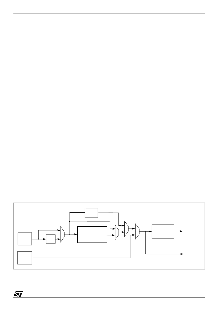
7.2.1 Clock Control Unit Overview
As shown in
Figure 59
a programmable divider
can divide the CLOCK1 input clock signal by two.
In practice, the divide-by-two is virtually always
used in order to ensure a 50% duty cycle signal to
Figure 59. Clock Control Unit Simplified Block Diagram
the PLL multiplier circuit. The resulting signal,
CLOCK2, is the reference input clock to the pro-
grammable Phase Locked Loop frequency multi-
plier, which is capable of multiplying the clock fre-
quency by a factor of 6, 8, 10 or 14; the multiplied
clock is then divided by a programmable divider,
by a factor of 1 to 7. By
these means, the ST9 can
operate with cheaper, medium frequency (3-5
MHz) crystals, while still providing a high frequen-
cy internal clock for maximum system perform-
ance; the range of available multiplication and divi-
sion factors allow a great number of operating
clock frequencies to be derived from a single crys-
tal frequency.
For low power operation, especially in Wait for In-
terrupt mode, the Clock Multiplier unit may be
turned off, whereupon the output clock signal may
be programmed as CLOCK2 divided by 16. For
further power reduction, a low frequency external
clock connected to the CK_AF pin may be select-
ed, whereupon the crystal controlled main oscilla-
tor may be turned off.
The internal system clock, INTCLK, is routed to all
on-chip peripherals, as well as to the programma-
ble Clock Prescaler Unit which generates the clock
for the CPU core (CPUCLK). (See
Figure 59
)
The Clock Prescaler is programmable and can
slow the CPU clock by a factor of up to 8, allowing
the programmer to reduce CPU processing speed,
and thus power consumption, while maintaining a
high speed clock to the peripherals. This is partic-
ularly useful when little actual processing is being
done by the CPU and the peripherals are doing
most of the work.
Crystal
oscillator
CK_AF
source
1/16
1/2
CLOCK2
CLOCK1
CK_AF
PLL
Clock Multiplier
/Divider
CPU Clock
Prescaler
to
CPU Core
to
Peripherals
CPUCLK
INTCLK
Unit
9
相关PDF资料 |
PDF描述 |
|---|---|
| ST92F250DR9Q6 | 8/16-BIT SINGLE VOLTAGE FLASH MCU FAMILY WITH RAM, E3 TMEMULATED EEPROM, CAN 2.0B AND J1850 BLPD |
| ST92250DV9QB | 8/16-BIT SINGLE VOLTAGE FLASH MCU FAMILY WITH RAM, E3 TMEMULATED EEPROM, CAN 2.0B AND J1850 BLPD |
| ST92F250DV9QB | 8/16-BIT SINGLE VOLTAGE FLASH MCU FAMILY WITH RAM, E3 TMEMULATED EEPROM, CAN 2.0B AND J1850 BLPD |
| ST92124JDV9QB | 8/16-BIT SINGLE VOLTAGE FLASH MCU FAMILY WITH RAM, E3 TMEMULATED EEPROM, CAN 2.0B AND J1850 BLPD |
| ST92F124JDV9QB | 8/16-BIT SINGLE VOLTAGE FLASH MCU FAMILY WITH RAM, E3 TMEMULATED EEPROM, CAN 2.0B AND J1850 BLPD |
相关代理商/技术参数 |
参数描述 |
|---|---|
| ST9250410AS | 制造商:Seagate Technology 功能描述:250GB 2.5" Momentus 5400.6 Mobile Hard Drive 制造商:Seagate Technology 功能描述:250GB 2.5" SATA Hard Drive 7200RPM |
| ST9250610NS | 制造商:Seagate Technology 功能描述:CONSTELLATION.2 2.5 250GB SATA 7200 NS 6GB/S - Bulk |
| ST-9258 | 制造商:UNBRANDED 功能描述:THERMOMETER DIGITAL 制造商:UNBRANDED 功能描述:THERMOMETER, DIGITAL |
| ST92916A681JPI | 制造商:ST MICRO 功能描述:New |
| ST92E141-EPB/US | 功能描述:程序设计器 - 基于处理器 ST9 EPROM Programmer RoHS:否 制造商:Olimex Ltd. 产品:Programmers 工具用于评估:XMEGA, MegaAVR, tinyAVR 核心:AVR 接口类型:USB 工作电源电压:1.8 V to 5.5 V |
发布紧急采购,3分钟左右您将得到回复。