- 您现在的位置:买卖IC网 > PDF目录380740 > ST92250DV9Q6 (意法半导体) 8/16-BIT SINGLE VOLTAGE FLASH MCU FAMILY WITH RAM, E3 TMEMULATED EEPROM, CAN 2.0B AND J1850 BLPD PDF资料下载
参数资料
| 型号: | ST92250DV9Q6 |
| 厂商: | 意法半导体 |
| 英文描述: | 8/16-BIT SINGLE VOLTAGE FLASH MCU FAMILY WITH RAM, E3 TMEMULATED EEPROM, CAN 2.0B AND J1850 BLPD |
| 中文描述: | 16位产品单电压闪存MCU的家庭的RAM,EEPROM的E3展TMEMULATED,可以2.0b和J1850 BLPD |
| 文件页数: | 60/426页 |
| 文件大小: | 3831K |
| 代理商: | ST92250DV9Q6 |
第1页第2页第3页第4页第5页第6页第7页第8页第9页第10页第11页第12页第13页第14页第15页第16页第17页第18页第19页第20页第21页第22页第23页第24页第25页第26页第27页第28页第29页第30页第31页第32页第33页第34页第35页第36页第37页第38页第39页第40页第41页第42页第43页第44页第45页第46页第47页第48页第49页第50页第51页第52页第53页第54页第55页第56页第57页第58页第59页当前第60页第61页第62页第63页第64页第65页第66页第67页第68页第69页第70页第71页第72页第73页第74页第75页第76页第77页第78页第79页第80页第81页第82页第83页第84页第85页第86页第87页第88页第89页第90页第91页第92页第93页第94页第95页第96页第97页第98页第99页第100页第101页第102页第103页第104页第105页第106页第107页第108页第109页第110页第111页第112页第113页第114页第115页第116页第117页第118页第119页第120页第121页第122页第123页第124页第125页第126页第127页第128页第129页第130页第131页第132页第133页第134页第135页第136页第137页第138页第139页第140页第141页第142页第143页第144页第145页第146页第147页第148页第149页第150页第151页第152页第153页第154页第155页第156页第157页第158页第159页第160页第161页第162页第163页第164页第165页第166页第167页第168页第169页第170页第171页第172页第173页第174页第175页第176页第177页第178页第179页第180页第181页第182页第183页第184页第185页第186页第187页第188页第189页第190页第191页第192页第193页第194页第195页第196页第197页第198页第199页第200页第201页第202页第203页第204页第205页第206页第207页第208页第209页第210页第211页第212页第213页第214页第215页第216页第217页第218页第219页第220页第221页第222页第223页第224页第225页第226页第227页第228页第229页第230页第231页第232页第233页第234页第235页第236页第237页第238页第239页第240页第241页第242页第243页第244页第245页第246页第247页第248页第249页第250页第251页第252页第253页第254页第255页第256页第257页第258页第259页第260页第261页第262页第263页第264页第265页第266页第267页第268页第269页第270页第271页第272页第273页第274页第275页第276页第277页第278页第279页第280页第281页第282页第283页第284页第285页第286页第287页第288页第289页第290页第291页第292页第293页第294页第295页第296页第297页第298页第299页第300页第301页第302页第303页第304页第305页第306页第307页第308页第309页第310页第311页第312页第313页第314页第315页第316页第317页第318页第319页第320页第321页第322页第323页第324页第325页第326页第327页第328页第329页第330页第331页第332页第333页第334页第335页第336页第337页第338页第339页第340页第341页第342页第343页第344页第345页第346页第347页第348页第349页第350页第351页第352页第353页第354页第355页第356页第357页第358页第359页第360页第361页第362页第363页第364页第365页第366页第367页第368页第369页第370页第371页第372页第373页第374页第375页第376页第377页第378页第379页第380页第381页第382页第383页第384页第385页第386页第387页第388页第389页第390页第391页第392页第393页第394页第395页第396页第397页第398页第399页第400页第401页第402页第403页第404页第405页第406页第407页第408页第409页第410页第411页第412页第413页第414页第415页第416页第417页第418页第419页第420页第421页第422页第423页第424页第425页第426页
60/426
ST92F124/F150/F250 - SINGLE VOLTAGE FLASH & E3 TM (EMULATED EEPROM)
3.5 PROTECTION STRATEGY
The protection bits are stored in the 4 locations
from 231FFCh to 231FFFh (see
Figure 34
).
All the available protections are forced active dur-
ing reset, then in the initialisation phase they are
read from the TestFlash.
The protections are stored in 2 Non Volatile Regis-
ters. Other 2 Non Volatile Registers can be used
as a password to re-enable test modes once they
have been disabled.
The protections can be programmed using the Set
Protection operation (see Control Registers para-
graph), that can be executed from all the internal
or external memories except the Flash or Test-
Flash itself.
The TestFlash area (230000h to 231F7Fh) is al-
ways protected against write access.
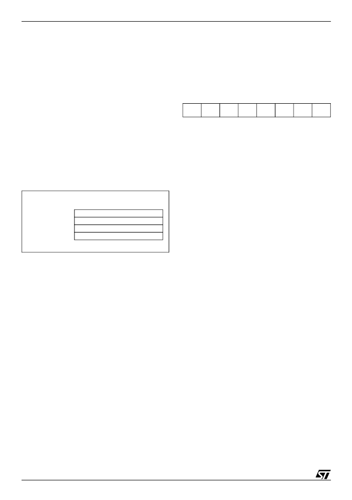
Figure 34. Protection Register Map
3.5.1 Non Volatile Registers
The 4 Non Volatile Registers used to store the pro-
tection bits for the different protection features are
one time programmable by the user.
Access to these registers is controlled by the pro-
tections related to the TestFlash. Since the code to
program the Protection Registers cannot be
fetched by the Flash or the TestFlash memories,
this means that, once the APRO or APBR bits in
the NVAPR register are programmed, it is no long-
er possible to modify any of the protection bits. For
this reason the NV Password, if needed, must be
set with the same Set Protection operation used to
program these bits. For the same reason it is
strongly advised to never program the WPBR bit in
the NVWPR register, as this will prevent any fur-
ther write access to the TestFlash, and conse-
quently to the Protection Registers.
NON VOLATILE ACCESS PROTECTION REG-
ISTER (NVAPR)
Address: 231FFCh - Read/Write
Delivery value: 1111 1111 (FFh)
Bit 7 = Reserved
.
Bit 6 =
APRO
:
FLASH access protection.
This bit, if programmed at 0, disables any access
(read/write) to operands mapped inside the Flash
address space (
E
3 TM
excluded), unless the current
instruction is fetched from the TestFlash or from
the Flash itself.
0: ROM protection on
1: ROM protection off
Bit 5 =
APBR
:
TestFlash access protection.
This bit, if programmed at 0, disables any access
(read/write) to operands mapped inside the Test-
Flash, the OTP and the protection registers, un-
less the current instruction is fetched from the
TestFlash or the OTP area.
0: TestFlash protection on
1: TestFlash protection off
Bit 4 =
APEE
:
E
3 TM
access protection.
This bit, if programmed at 0, disables any access
(read/write) to operands mapped inside the
E
3 TM
address space, unless the current instruction is
fetched from the TestFlash or from the Flash, or
from the
E
3 TM
itself.
0:
E
3 TM
protection on
1:
E
3 TM
protection off
Bit 3 =
APEX
:
Access Protection from External
memory.
This bit, if programmed at 0, disables any access
(read/write) to operands mapped inside the ad-
dress space of one of the internal memories (Test-
Flash, Flash,
E
3 TM
, RAM), if the current instruction
is fetched from an external memory.
0: Protection from external memory on
1: Protection from external memory off
NVAPR
NVWPR
NVPWD0
NVPWD1
231FFCh
231FFDh
231FFEh
231FFFh
7
6
5
4
3
2
1
0
1
APRO APBR
APEE
APEX
PWT2 PWT1 PWT0
9
相关PDF资料 |
PDF描述 |
|---|---|
| ST92F250DV9Q6 | 8/16-BIT SINGLE VOLTAGE FLASH MCU FAMILY WITH RAM, E3 TMEMULATED EEPROM, CAN 2.0B AND J1850 BLPD |
| ST92124JDV9Q6 | 8/16-BIT SINGLE VOLTAGE FLASH MCU FAMILY WITH RAM, E3 TMEMULATED EEPROM, CAN 2.0B AND J1850 BLPD |
| ST92F124JDV9Q6 | 8/16-BIT SINGLE VOLTAGE FLASH MCU FAMILY WITH RAM, E3 TMEMULATED EEPROM, CAN 2.0B AND J1850 BLPD |
| ST92250JDV9Q6 | 8/16-BIT SINGLE VOLTAGE FLASH MCU FAMILY WITH RAM, E3 TMEMULATED EEPROM, CAN 2.0B AND J1850 BLPD |
| ST92F250JDV9Q6 | 8/16-BIT SINGLE VOLTAGE FLASH MCU FAMILY WITH RAM, E3 TMEMULATED EEPROM, CAN 2.0B AND J1850 BLPD |
相关代理商/技术参数 |
参数描述 |
|---|---|
| ST9250410AS | 制造商:Seagate Technology 功能描述:250GB 2.5" Momentus 5400.6 Mobile Hard Drive 制造商:Seagate Technology 功能描述:250GB 2.5" SATA Hard Drive 7200RPM |
| ST9250610NS | 制造商:Seagate Technology 功能描述:CONSTELLATION.2 2.5 250GB SATA 7200 NS 6GB/S - Bulk |
| ST-9258 | 制造商:UNBRANDED 功能描述:THERMOMETER DIGITAL 制造商:UNBRANDED 功能描述:THERMOMETER, DIGITAL |
| ST92916A681JPI | 制造商:ST MICRO 功能描述:New |
| ST92E141-EPB/US | 功能描述:程序设计器 - 基于处理器 ST9 EPROM Programmer RoHS:否 制造商:Olimex Ltd. 产品:Programmers 工具用于评估:XMEGA, MegaAVR, tinyAVR 核心:AVR 接口类型:USB 工作电源电压:1.8 V to 5.5 V |
发布紧急采购,3分钟左右您将得到回复。