- 您现在的位置:买卖IC网 > PDF目录380740 > ST92250JDV9QB (意法半导体) 8/16-BIT SINGLE VOLTAGE FLASH MCU FAMILY WITH RAM, E3 TMEMULATED EEPROM, CAN 2.0B AND J1850 BLPD PDF资料下载
参数资料
| 型号: | ST92250JDV9QB |
| 厂商: | 意法半导体 |
| 英文描述: | 8/16-BIT SINGLE VOLTAGE FLASH MCU FAMILY WITH RAM, E3 TMEMULATED EEPROM, CAN 2.0B AND J1850 BLPD |
| 中文描述: | 16位产品单电压闪存MCU的家庭的RAM,EEPROM的E3展TMEMULATED,可以2.0b和J1850 BLPD |
| 文件页数: | 58/426页 |
| 文件大小: | 3831K |
| 代理商: | ST92250JDV9QB |
第1页第2页第3页第4页第5页第6页第7页第8页第9页第10页第11页第12页第13页第14页第15页第16页第17页第18页第19页第20页第21页第22页第23页第24页第25页第26页第27页第28页第29页第30页第31页第32页第33页第34页第35页第36页第37页第38页第39页第40页第41页第42页第43页第44页第45页第46页第47页第48页第49页第50页第51页第52页第53页第54页第55页第56页第57页当前第58页第59页第60页第61页第62页第63页第64页第65页第66页第67页第68页第69页第70页第71页第72页第73页第74页第75页第76页第77页第78页第79页第80页第81页第82页第83页第84页第85页第86页第87页第88页第89页第90页第91页第92页第93页第94页第95页第96页第97页第98页第99页第100页第101页第102页第103页第104页第105页第106页第107页第108页第109页第110页第111页第112页第113页第114页第115页第116页第117页第118页第119页第120页第121页第122页第123页第124页第125页第126页第127页第128页第129页第130页第131页第132页第133页第134页第135页第136页第137页第138页第139页第140页第141页第142页第143页第144页第145页第146页第147页第148页第149页第150页第151页第152页第153页第154页第155页第156页第157页第158页第159页第160页第161页第162页第163页第164页第165页第166页第167页第168页第169页第170页第171页第172页第173页第174页第175页第176页第177页第178页第179页第180页第181页第182页第183页第184页第185页第186页第187页第188页第189页第190页第191页第192页第193页第194页第195页第196页第197页第198页第199页第200页第201页第202页第203页第204页第205页第206页第207页第208页第209页第210页第211页第212页第213页第214页第215页第216页第217页第218页第219页第220页第221页第222页第223页第224页第225页第226页第227页第228页第229页第230页第231页第232页第233页第234页第235页第236页第237页第238页第239页第240页第241页第242页第243页第244页第245页第246页第247页第248页第249页第250页第251页第252页第253页第254页第255页第256页第257页第258页第259页第260页第261页第262页第263页第264页第265页第266页第267页第268页第269页第270页第271页第272页第273页第274页第275页第276页第277页第278页第279页第280页第281页第282页第283页第284页第285页第286页第287页第288页第289页第290页第291页第292页第293页第294页第295页第296页第297页第298页第299页第300页第301页第302页第303页第304页第305页第306页第307页第308页第309页第310页第311页第312页第313页第314页第315页第316页第317页第318页第319页第320页第321页第322页第323页第324页第325页第326页第327页第328页第329页第330页第331页第332页第333页第334页第335页第336页第337页第338页第339页第340页第341页第342页第343页第344页第345页第346页第347页第348页第349页第350页第351页第352页第353页第354页第355页第356页第357页第358页第359页第360页第361页第362页第363页第364页第365页第366页第367页第368页第369页第370页第371页第372页第373页第374页第375页第376页第377页第378页第379页第380页第381页第382页第383页第384页第385页第386页第387页第388页第389页第390页第391页第392页第393页第394页第395页第396页第397页第398页第399页第400页第401页第402页第403页第404页第405页第406页第407页第408页第409页第410页第411页第412页第413页第414页第415页第416页第417页第418页第419页第420页第421页第422页第423页第424页第425页第426页
58/426
ST92F124/F150/F250 - SINGLE VOLTAGE FLASH & E3 TM (EMULATED EEPROM)
REGISTER DESCRIPTION
(Cont’d)
The meaning of the FESSx bit for sector x is given
in
Table 10
.
FLASH &
E
3 TM
STATUS REGISTER 1
(FESR1)
Address: 224003h /221003h-Read Only
Reset value: 0000 0000 (00h)
Bit 7 =
ERER
.
Erase error (Read Only).
This bit is set by hardware when an Erase error oc-
curs during a Flash or an
E
3 TM
write operation.
This error is due to a real failure of a Flash cell,
that can no longer be erased. This kind of error is
fatal and the sector where it occurred must be dis-
carded. This bit is automatically cleared when bit
FEERR of the FESR0 register is cleared by soft-
ware.
0: Erase OK
1: Erase error
Bit 6 =
PGER
.
Program error (Read Only).
This bit is automatically set when a Program error
occurs during a Flash or an
E
3 TM
write operation.
This error is due to a real failure of a Flash cell,
that can no longer be programmed. The byte
where this error occurred must be discarded (if it
was in the
E
3 TM
memory, the byte must be repro-
grammed to FFh and then discarded, to avoid the
error occurring again when that byte is internally
moved). This bit is automatically cleared when bit
FEERR of the FESR0 register is cleared by soft-
ware.
0: Program OK
1: Flash or
E
3 TM
Programming error
Bit 5 =
SWER
.
Swap or 1 over 0 Error (Read On-
ly).
This bit has two different meanings, depending on
whether the current write operation is to Flash or
E
3 TM
memory.
In Flash memory this bit is automatically set when
trying to program at 1 bits previously set at 0 (this
does not happen when programming the Protec-
tion bits). This error is not due to a failure of the
Flash cell, but only flags that the desired data has
not been written.
In the
E
3 TM
memory this bit is automatically set
when a Program error occurs during the swapping
of the unselected pages to the new sector when
the old sector is full (see AN1152 for more details).
This error is due to a real failure of a Flash cell,
that can no longer be programmed. When this er-
ror is detected, the embedded algorithm automati-
cally exits the Page Update operation at the end of
the Swap phase, without performing the Erase
Phase 0 on the full sector. In this way the old data
are kept, and through predefined routines in Test-
Flash (Find Wrong Pages = 230029h and Find
Wrong Bytes = 23002Ch), the user can compare
the old and the new data to find where the error oc-
curred.
Once the error has been discovered the user must
take to end the stopped Erase Phase 0 on the old
sector (through another predefined routine in Test-
Flash
:
Complete Swap = 23002Fh). The byte
where the error occurred must be reprogrammed
to FFh and then discarded, to avoid the error oc-
curring again when that byte is internally moved.
This bit is automatically cleared when bit FEERR
of the FESR0 register is cleared by software.
Bit 4:0 = Reserved.
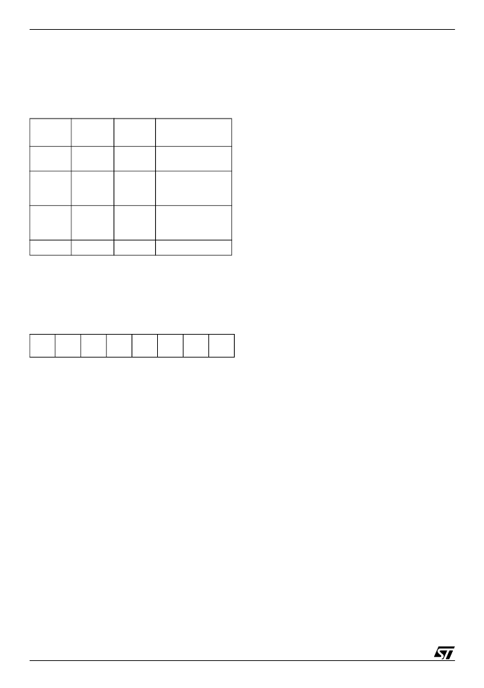
Table 10. Sector Status Bits
FEERR
FBUSY
EBUSY
FSUSP
FESSx=1
meaning
1
-
-
Write Error in
Sector x
0
1
-
Write operation
on-going in sec-
tor x
0
0
1
Sector Erase
Suspended in
sector x
0
0
0
Don’t care
7
6
5
4
3
2
1
0
ERER PGER SWER
9
相关PDF资料 |
PDF描述 |
|---|---|
| ST92F250JDV9QB | 8/16-BIT SINGLE VOLTAGE FLASH MCU FAMILY WITH RAM, E3 TMEMULATED EEPROM, CAN 2.0B AND J1850 BLPD |
| ST92150DV9QC | 8/16-BIT SINGLE VOLTAGE FLASH MCU FAMILY WITH RAM, E3 TMEMULATED EEPROM, CAN 2.0B AND J1850 BLPD |
| ST92F150DV9QC | 8/16-BIT SINGLE VOLTAGE FLASH MCU FAMILY WITH RAM, E3 TMEMULATED EEPROM, CAN 2.0B AND J1850 BLPD |
| ST92150JDV9QC | 8/16-BIT SINGLE VOLTAGE FLASH MCU FAMILY WITH RAM, E3 TMEMULATED EEPROM, CAN 2.0B AND J1850 BLPD |
| ST92F150JDV9QC | 8/16-BIT SINGLE VOLTAGE FLASH MCU FAMILY WITH RAM, E3 TMEMULATED EEPROM, CAN 2.0B AND J1850 BLPD |
相关代理商/技术参数 |
参数描述 |
|---|---|
| ST9250410AS | 制造商:Seagate Technology 功能描述:250GB 2.5" Momentus 5400.6 Mobile Hard Drive 制造商:Seagate Technology 功能描述:250GB 2.5" SATA Hard Drive 7200RPM |
| ST9250610NS | 制造商:Seagate Technology 功能描述:CONSTELLATION.2 2.5 250GB SATA 7200 NS 6GB/S - Bulk |
| ST-9258 | 制造商:UNBRANDED 功能描述:THERMOMETER DIGITAL 制造商:UNBRANDED 功能描述:THERMOMETER, DIGITAL |
| ST92916A681JPI | 制造商:ST MICRO 功能描述:New |
| ST92E141-EPB/US | 功能描述:程序设计器 - 基于处理器 ST9 EPROM Programmer RoHS:否 制造商:Olimex Ltd. 产品:Programmers 工具用于评估:XMEGA, MegaAVR, tinyAVR 核心:AVR 接口类型:USB 工作电源电压:1.8 V to 5.5 V |
发布紧急采购,3分钟左右您将得到回复。