- 您现在的位置:买卖IC网 > PDF目录380749 > ST92F250CR9T6 (意法半导体) 8/16-BIT SINGLE VOLTAGE FLASH MCU FAMILY WITH RAM, E3 TMEMULATED EEPROM, CAN 2.0B AND J1850 BLPD PDF资料下载
参数资料
| 型号: | ST92F250CR9T6 |
| 厂商: | 意法半导体 |
| 英文描述: | 8/16-BIT SINGLE VOLTAGE FLASH MCU FAMILY WITH RAM, E3 TMEMULATED EEPROM, CAN 2.0B AND J1850 BLPD |
| 中文描述: | 16位产品单电压闪存MCU的家庭的RAM,EEPROM的E3展TMEMULATED,可以2.0b和J1850 BLPD |
| 文件页数: | 150/426页 |
| 文件大小: | 3831K |
| 代理商: | ST92F250CR9T6 |
第1页第2页第3页第4页第5页第6页第7页第8页第9页第10页第11页第12页第13页第14页第15页第16页第17页第18页第19页第20页第21页第22页第23页第24页第25页第26页第27页第28页第29页第30页第31页第32页第33页第34页第35页第36页第37页第38页第39页第40页第41页第42页第43页第44页第45页第46页第47页第48页第49页第50页第51页第52页第53页第54页第55页第56页第57页第58页第59页第60页第61页第62页第63页第64页第65页第66页第67页第68页第69页第70页第71页第72页第73页第74页第75页第76页第77页第78页第79页第80页第81页第82页第83页第84页第85页第86页第87页第88页第89页第90页第91页第92页第93页第94页第95页第96页第97页第98页第99页第100页第101页第102页第103页第104页第105页第106页第107页第108页第109页第110页第111页第112页第113页第114页第115页第116页第117页第118页第119页第120页第121页第122页第123页第124页第125页第126页第127页第128页第129页第130页第131页第132页第133页第134页第135页第136页第137页第138页第139页第140页第141页第142页第143页第144页第145页第146页第147页第148页第149页当前第150页第151页第152页第153页第154页第155页第156页第157页第158页第159页第160页第161页第162页第163页第164页第165页第166页第167页第168页第169页第170页第171页第172页第173页第174页第175页第176页第177页第178页第179页第180页第181页第182页第183页第184页第185页第186页第187页第188页第189页第190页第191页第192页第193页第194页第195页第196页第197页第198页第199页第200页第201页第202页第203页第204页第205页第206页第207页第208页第209页第210页第211页第212页第213页第214页第215页第216页第217页第218页第219页第220页第221页第222页第223页第224页第225页第226页第227页第228页第229页第230页第231页第232页第233页第234页第235页第236页第237页第238页第239页第240页第241页第242页第243页第244页第245页第246页第247页第248页第249页第250页第251页第252页第253页第254页第255页第256页第257页第258页第259页第260页第261页第262页第263页第264页第265页第266页第267页第268页第269页第270页第271页第272页第273页第274页第275页第276页第277页第278页第279页第280页第281页第282页第283页第284页第285页第286页第287页第288页第289页第290页第291页第292页第293页第294页第295页第296页第297页第298页第299页第300页第301页第302页第303页第304页第305页第306页第307页第308页第309页第310页第311页第312页第313页第314页第315页第316页第317页第318页第319页第320页第321页第322页第323页第324页第325页第326页第327页第328页第329页第330页第331页第332页第333页第334页第335页第336页第337页第338页第339页第340页第341页第342页第343页第344页第345页第346页第347页第348页第349页第350页第351页第352页第353页第354页第355页第356页第357页第358页第359页第360页第361页第362页第363页第364页第365页第366页第367页第368页第369页第370页第371页第372页第373页第374页第375页第376页第377页第378页第379页第380页第381页第382页第383页第384页第385页第386页第387页第388页第389页第390页第391页第392页第393页第394页第395页第396页第397页第398页第399页第400页第401页第402页第403页第404页第405页第406页第407页第408页第409页第410页第411页第412页第413页第414页第415页第416页第417页第418页第419页第420页第421页第422页第423页第424页第425页第426页
150/426
ST92F124/F150/F250 - I/O PORTS
9 I/O PORTS
9.1 INTRODUCTION
ST9 devices feature flexible individually program-
mable multifunctional input/output lines. Refer to
the Pin Description Chapter for specific pin alloca-
tions. These lines, which are logically grouped as
8-bit ports, can be individually programmed to pro-
vide digital input/output and analog input, or to
connect input/output signals to the on-chip periph-
erals as alternate pin functions. All ports can be in-
dividually configured as an input, bi-directional,
output or alternate function. In addition, pull-ups
can be turned off for open-drain operation, and
weak pull-ups can be turned on in their place, to
avoid the need for off-chip resistive pull-ups. Ports
configured as open drain must never have voltage
on the port pin exceeding V
DD
(refer to the Electri-
cal Characteristics section). Depending on the
specific port, input buffers are software selectable
to be TTL or CMOS compatible, however on Sch-
mitt trigger ports, no selection is possible.
9.2 SPECIFIC PORT CONFIGURATIONS
Refer to the Pin Description chapter for a list of the
specific port styles and reset values.
9.3 PORT CONTROL REGISTERS
Each port is associated with a Data register
(PxDR) and three Control registers (PxC0, PxC1,
PxC2). These define the port configuration and al-
low dynamic configuration changes during pro-
gram execution. Port Data and Control registers
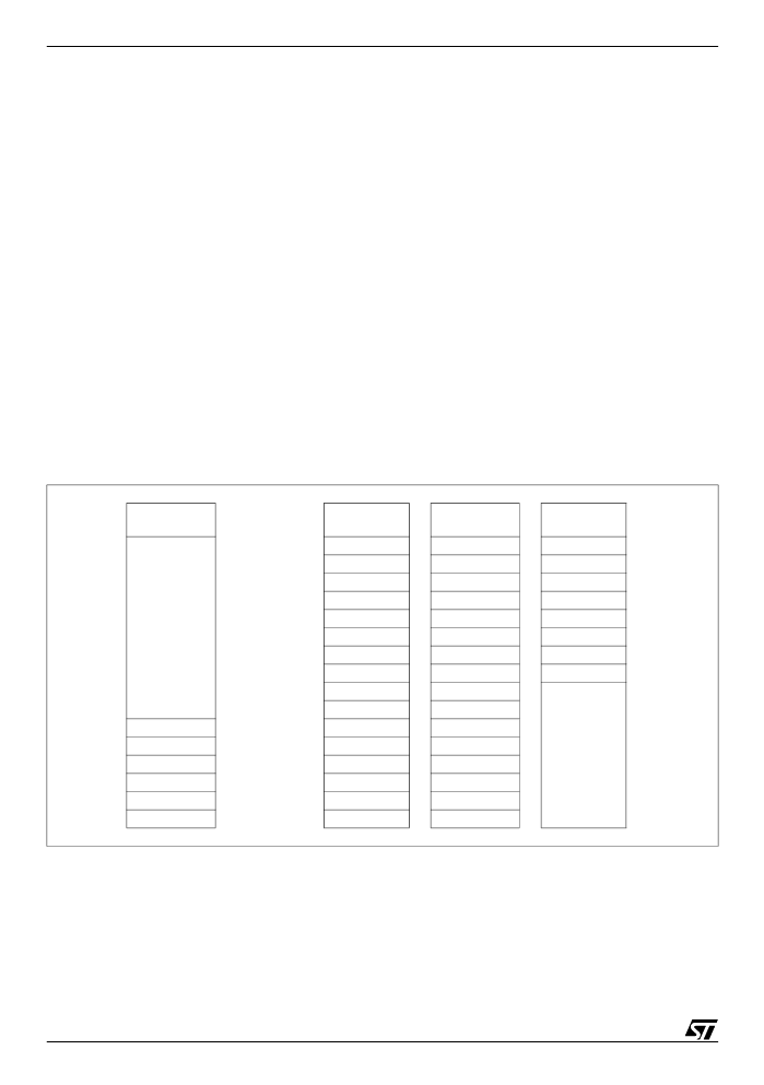
are mapped into the Register File as shown in
Fig-
ure 79
. Port Data and Control registers are treated
just like any other general purpose register. There
are no special instructions for port manipulation:
any instruction that can address a register, can ad-
dress the ports. Data can be directly accessed in
the port register, without passing through other
memory or “accumulator” locations.
Figure 79. I/O Register Map
GROUP E
GROUP F
PAGE 2
Reserved
P3C2
P3C1
P3C0
Reserved
P2C2
P2C1
P2C0
Reserved
P1C2
P1C1
P1C0
Reserved
P0C2
P0C1
P0C0
GROUP F
PAGE 3
P7DR
P7C2
P7C1
P7C0
P6DR
P6C2
P6C1
P6C0
Reserved
P5C2
P5C1
P5C0
Reserved
P4C2
P4C1
P4C0
GROUP F
PAGE 43
P9DR
P9C2
P9C1
P9C0
P8DR
P8C2
P8C1
P8C0
System
Registers
FFh
FEh
FDh
FCh
FBh
FAh
F9h
F8h
F7h
F6h
F5h
F4h
F3h
F2h
F1h
F0h
R255
R254
R253
R252
R251
R250
R249
R248
R247
R246
R245
R244
R243
R242
R241
R240
Reserved
E5h
E4h
E3h
E2h
E1h
E0h
P5DR
P4DR
P3DR
P2DR
P1DR
P0DR
R229
R228
R227
R226
R225
R224
9
相关PDF资料 |
PDF描述 |
|---|---|
| ST92F250CR9TB | 8/16-BIT SINGLE VOLTAGE FLASH MCU FAMILY WITH RAM, E3 TMEMULATED EEPROM, CAN 2.0B AND J1850 BLPD |
| ST92F250CR9TC | 8/16-BIT SINGLE VOLTAGE FLASH MCU FAMILY WITH RAM, E3 TMEMULATED EEPROM, CAN 2.0B AND J1850 BLPD |
| ST92F250CV1QB | 8/16-BIT SINGLE VOLTAGE FLASH MCU FAMILY WITH RAM, E3 TMEMULATED EEPROM, CAN 2.0B AND J1850 BLPD |
| ST92F250CV1QC | 8/16-BIT SINGLE VOLTAGE FLASH MCU FAMILY WITH RAM, E3 TMEMULATED EEPROM, CAN 2.0B AND J1850 BLPD |
| ST92F250CV1T6 | 8/16-BIT SINGLE VOLTAGE FLASH MCU FAMILY WITH RAM, E3 TMEMULATED EEPROM, CAN 2.0B AND J1850 BLPD |
相关代理商/技术参数 |
参数描述 |
|---|---|
| ST92F250CV2QB | 功能描述:8位微控制器 -MCU 256K Flash 8K RAM RoHS:否 制造商:Silicon Labs 核心:8051 处理器系列:C8051F39x 数据总线宽度:8 bit 最大时钟频率:50 MHz 程序存储器大小:16 KB 数据 RAM 大小:1 KB 片上 ADC:Yes 工作电源电压:1.8 V to 3.6 V 工作温度范围:- 40 C to + 105 C 封装 / 箱体:QFN-20 安装风格:SMD/SMT |
| ST92F250CV2TB | 功能描述:8位微控制器 -MCU 256K Flash 8K RAM RoHS:否 制造商:Silicon Labs 核心:8051 处理器系列:C8051F39x 数据总线宽度:8 bit 最大时钟频率:50 MHz 程序存储器大小:16 KB 数据 RAM 大小:1 KB 片上 ADC:Yes 工作电源电压:1.8 V to 3.6 V 工作温度范围:- 40 C to + 105 C 封装 / 箱体:QFN-20 安装风格:SMD/SMT |
| ST92F250CV2TBE | 制造商:STMicroelectronics 功能描述:MCU 8-bit/16-bit ST92 CISC 256KB Flash 5V 100-Pin LQFP Tray |
| ST92T141K4B6 | 功能描述:8位微控制器 -MCU OTP EPROM 16K SPI RoHS:否 制造商:Silicon Labs 核心:8051 处理器系列:C8051F39x 数据总线宽度:8 bit 最大时钟频率:50 MHz 程序存储器大小:16 KB 数据 RAM 大小:1 KB 片上 ADC:Yes 工作电源电压:1.8 V to 3.6 V 工作温度范围:- 40 C to + 105 C 封装 / 箱体:QFN-20 安装风格:SMD/SMT |
| ST92T141K4M6 | 功能描述:8位微控制器 -MCU OTP EPROM 16K SPI RoHS:否 制造商:Silicon Labs 核心:8051 处理器系列:C8051F39x 数据总线宽度:8 bit 最大时钟频率:50 MHz 程序存储器大小:16 KB 数据 RAM 大小:1 KB 片上 ADC:Yes 工作电源电压:1.8 V to 3.6 V 工作温度范围:- 40 C to + 105 C 封装 / 箱体:QFN-20 安装风格:SMD/SMT |
发布紧急采购,3分钟左右您将得到回复。