- 您现在的位置:买卖IC网 > PDF目录374939 > STC62WV51216EIPO70 (Electronic Theatre Controls, Inc.) Very Low Power/Voltage CMOS SRAM PDF资料下载
参数资料
| 型号: | STC62WV51216EIPO70 |
| 厂商: | Electronic Theatre Controls, Inc. |
| 英文描述: | Very Low Power/Voltage CMOS SRAM |
| 中文描述: | 非常低功率/电压的CMOS的SRAM |
| 文件页数: | 2/10页 |
| 文件大小: | 385K |
| 代理商: | STC62WV51216EIPO70 |
Revision 2.3
Jan.
2004
2
STC
C
IN
Input
Capacitance
Input/Output
Capacitance
V
IN
=0V
6
pF
C
DQ
V
I/O
=0V
8
pF
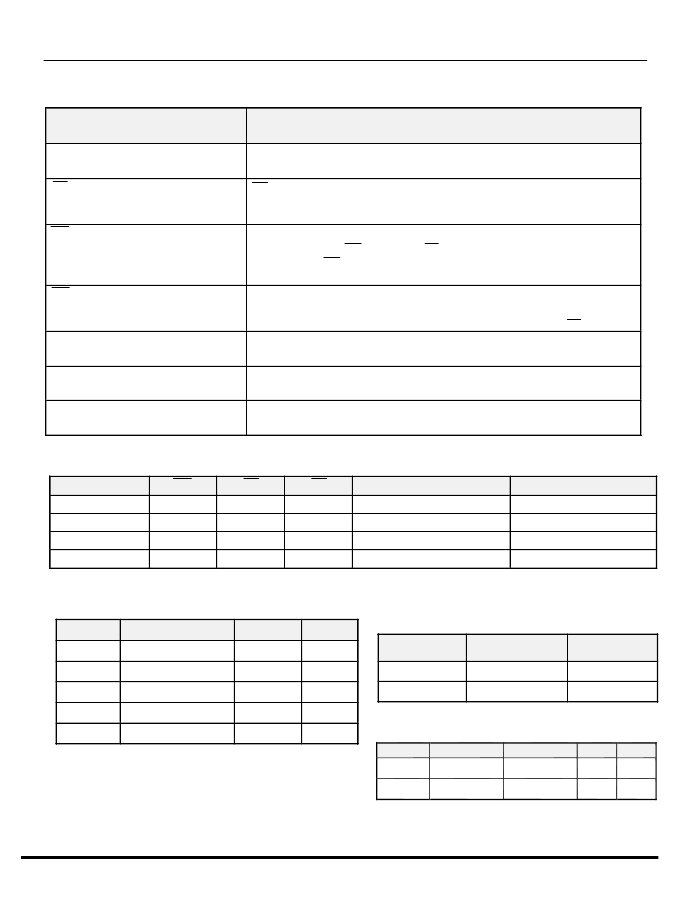
ABSOLUTE MAXIMUM RATINGS
(1)
OPERATING RANGE
CAPACITANCE
(1)
(TA = 25
o
C, f = 1.0 MHz)
1. Stresses greater than those listed under ABSOLUTE MAXIMUM
RATINGS may cause permanent damage to the device. This is a
stress rating only and functional operation of the device at these
or any other conditions above those indicated in the operational
sections of this specification is not implied. Exposure to absolute
maximum rating conditions for extended periods may affect
reliability.
1. This parameter is guaranteed and not 100% tested.
SYMBOL
PARAMETER
Terminal
Respect to GND
RATING
-0.5 to
Vcc+0.5
UNITS
V
TERM
Voltage
with
V
T
BIAS
Temperature Under Bias
-40 to +125
O
C
T
STG
Storage Temperature
-60 to +150
O
C
P
T
Power Dissipation
1.0
W
I
OUT
DC Output Current
20
mA
STC62WV256
RANGE
AMBIENT
TEMPERATURE
0
O
C to +70
O
C
Vcc
Commercial
2.4V ~ 5.5V
Industrial
-40
O
C to +85
O
C
2.4V ~ 5.5V
R0201-
STC62WV256
Name
Function
A0-A14 Address Input
These 15 address inputs select one of the 32768 x 8-bit words in the RAM
CE Chip Enable Input
CE is active LOW. Chip enables must be active when data read from or write to the
device. If chip enable is not active, the device is deselected and is in a standby power
mode. The DQ pins will be in the high impedance state when the device is deselected.
The write enable input is active LOW and controls read and write operations. With the
chip selected, when WE is HIGH and OE is LOW, output data will be present on the
DQ pins; when WE is LOW, the data present on the DQ pins will be written into the
selected memory location.
The output enable input is active LOW. If the output enable is active while the chip is
selected and the write enable is inactive, data will be present on the DQ pins and they
will be enabled. The DQ pins will be in the high impedance state when OE is inactive.
These 8 bi-directional ports are used to read data from or write data into the RAM.
WE Write Enable Input
OE Output Enable Input
DQ0 – DQ7 Data Input/Output
Ports
Vcc
Power Supply
Gnd
Ground
TRUTH TABLE
PIN DESCRIPTIONS
MODE
WE
CE
OE
I/O OPERATION
Vcc CURRENT
Not selected
Output Disabled
Read
Write
X
H
H
L
H
L
L
L
X
H
L
X
High Z
High Z
D
OUT
D
IN
I
CCSB
, I
CCSB1
I
CC
I
CC
I
CC
SYMBOL
PARAMETER
CONDITIONS
MAX.
UNIT
相关PDF资料 |
PDF描述 |
|---|---|
| STC62WV51216FC | Very Low Power/Voltage CMOS SRAM |
| STC62WV51216FCG55 | Very Low Power/Voltage CMOS SRAM |
| STC62WV51216FI | Very Low Power/Voltage CMOS SRAM |
| STC62WV51216FIP70 | Very Low Power/Voltage CMOS SRAM |
| STC62WV1024SCG70 | VERY LOW POWER VOLTAGE CMOS SRAM |
相关代理商/技术参数 |
参数描述 |
|---|---|
| STC62WV51216FC | 制造商:未知厂家 制造商全称:未知厂家 功能描述:Very Low Power/Voltage CMOS SRAM |
| STC62WV51216FCG55 | 制造商:未知厂家 制造商全称:未知厂家 功能描述:Very Low Power/Voltage CMOS SRAM |
| STC62WV51216FI | 制造商:未知厂家 制造商全称:未知厂家 功能描述:Very Low Power/Voltage CMOS SRAM |
| STC62WV51216FIP70 | 制造商:未知厂家 制造商全称:未知厂家 功能描述:Very Low Power/Voltage CMOS SRAM |
| STC62WV5128 | 制造商:未知厂家 制造商全称:未知厂家 功能描述:Very Low Power/Voltage CMOS SRAM |
发布紧急采购,3分钟左右您将得到回复。