- 您现在的位置:买卖IC网 > PDF目录98147 > STCD23100F35F (STMICROELECTRONICS) 2310 SERIES, LOW SKEW CLOCK DRIVER, 4 TRUE OUTPUT(S), 0 INVERTED OUTPUT(S), PBGA12 PDF资料下载
参数资料
| 型号: | STCD23100F35F |
| 厂商: | STMICROELECTRONICS |
| 元件分类: | 时钟及定时 |
| 英文描述: | 2310 SERIES, LOW SKEW CLOCK DRIVER, 4 TRUE OUTPUT(S), 0 INVERTED OUTPUT(S), PBGA12 |
| 封装: | 1.20 X 1.60 MM, 0.40 MM PITCH, ROHS COMPLIANT, FLIP CHIP-12 |
| 文件页数: | 24/39页 |
| 文件大小: | 1948K |
| 代理商: | STCD23100F35F |
第1页第2页第3页第4页第5页第6页第7页第8页第9页第10页第11页第12页第13页第14页第15页第16页第17页第18页第19页第20页第21页第22页第23页当前第24页第25页第26页第27页第28页第29页第30页第31页第32页第33页第34页第35页第36页第37页第38页第39页
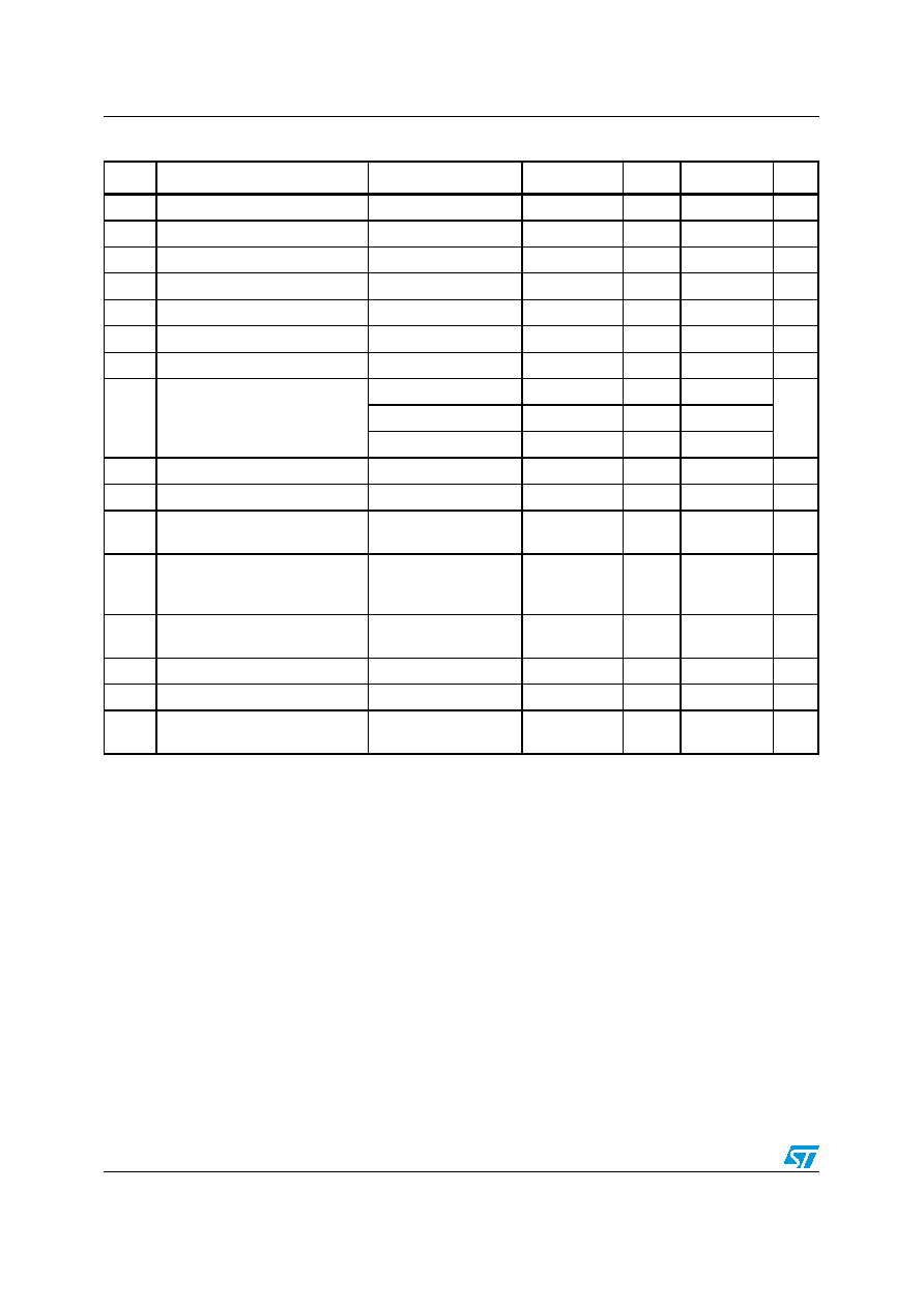
DC and AC parameters
STCD22x0, STCD23x0, STCD24x0
Doc ID 15400 Rev 2
CIN
Input capacitance
3
4
pF
IOO
Output to output isolation
45
dB
IOI
Output to input isolation
45
dB
VENH
Enable voltage high(9)
For EN1-EN4
1.2
V
VENL
Enable voltage low(9)
For EN1-EN4
0.6
V
VOPTH
OPT pins voltage high
For OPT1 and OPT2
VCC –0.3
VCC
V
VOPTL
OPT pins voltage low
For OPT1 and OPT2
GND
GND+0.3
V
PN
Additive phase noise(3)(10)
at 1 kHz offset
–135
dBc/
Hz
at 10 kHz offset
–145
at 100 kHz offset
–150
tJP
Additive period jitter(3)
rms value
10
ps
tJC
Additive cycle-cycle jitter(3)
rms value
10
ps
tRECB
Buffer recovery time from off to
on
STCD2xx0 active
1
10
s
tRECC
STCD2xx0 recovery time from
standby to active (include LDO
wakeup time)
500
s
tPD
Input to output propagation
delay(3)
Voltage transfer at 50%
3.5
6
ns
CL
Capacitive load for each channel
20
40
pF
RL
Resistive load for each channel
10
k
Ω
ZOUT
Output impedance for each
channel
50
Ω
1.
Valid for ambient operating temperature: TA = –20 °C to 85 °C; VCC = 2.5 V to 5.1 V; typical TA = 25 °C;
load capacitance = 20 pF, fMCLK = 26 MHz (except where noted).
2.
Total accuracy includes line and load regulation, temperature and process condition. It does not include load and line
transients.
3.
Simulated and determined via design and not 100% tested.
4.
Ripple voltage = 0.1 Vpp.
5.
Clock input voltage level should not exceed VTCXO voltage.
6.
The rise time is measured when clock edge transfers from 10% VCC to 90%VCC. The fall time is measured when clock
edge transfers from 90%VCC to 10%VCC. The output rise/fall time is guaranteed for all input slew rates.
7.
The quiescent current is measured when the enable pins are active, but with no input master clock signal (fMCLK = 0 Hz).
8.
The active current depends on the input master clock Vpp and frequency and the load condition. The typical test condition
is 26 MHz with 1.8 Vpp master clock input, CL = 20 pF.
9.
The test condition is VENH = 1.8 V and VENL = 0 V. When output enables simultaneously, there is no intentional skew in
design between the output clocks.
10. Guaranteed for all input clock slew rates.
Table 10.
DC and AC characteristics (continued)
Sym.
Parameter
Condition(1)
Min
Typ
Max
Unit
相关PDF资料 |
PDF描述 |
|---|---|
| STCL1120YBFCWY5 | 12 MHz, OTHER CLOCK GENERATOR, PDSO5 |
| STE10/100E | 1 CHANNEL(S), 100M bps, LOCAL AREA NETWORK CONTROLLER, PQFP128 |
| STEL-1173/CM | 8-BIT, DSP-NUM CONTROLLED OSCILLATOR, PQCC44 |
| STEL-1375A+80 | SPECIALTY MICROPROCESSOR CIRCUIT, DIP35 |
| STEL-1376 | SPECIALTY MICROPROCESSOR CIRCUIT, DIP65 |
相关代理商/技术参数 |
参数描述 |
|---|---|
| STCD2400 | 制造商:STMICROELECTRONICS 制造商全称:STMicroelectronics 功能描述:Multichannel clock distribution circuit |
| STCD2400F35F | 功能描述:MOSFET Multichannel Clock 1.8V RF 40pF RoHS:否 制造商:STMicroelectronics 晶体管极性:N-Channel 汲极/源极击穿电压:650 V 闸/源击穿电压:25 V 漏极连续电流:130 A 电阻汲极/源极 RDS(导通):0.014 Ohms 配置:Single 最大工作温度: 安装风格:Through Hole 封装 / 箱体:Max247 封装:Tube |
| STCD500100 | 制造商:Seagate Technology 功能描述:SEAGATE SLIM - Trays 制造商:Seagate Technology 功能描述:500GB Slim Portable USB 3.0 External Hard Drive |
| STCD500102 | 制造商:Seagate Technology 功能描述:SEAGATE SLIM (COBRA), BLACK USB 3.0 500GB - Trays |
| STCD500104 | 制造商:Seagate Technology 功能描述:500GB Backup Plus Portable USB 3.0 External Hard Drive Silver |
发布紧急采购,3分钟左右您将得到回复。