- 您现在的位置:买卖IC网 > PDF目录98148 > STK17TA8-R45 REAL TIME CLOCK, PDSO48 PDF资料下载
参数资料
| 型号: | STK17TA8-R45 |
| 元件分类: | 时钟/数据恢复及定时提取 |
| 英文描述: | REAL TIME CLOCK, PDSO48 |
| 封装: | 0.300 INCH, 0.025 INCH PITCH, PLASTIC, SSOP-48 |
| 文件页数: | 10/25页 |
| 文件大小: | 285K |
| 代理商: | STK17TA8-R45 |
STK17TA8
April 2005
Document Control #ML0025 rev 1.1
18
the user after tHRECALL delay (See AutoStore
/POWER-UP RECALL) after VCC has been restored
to the device.
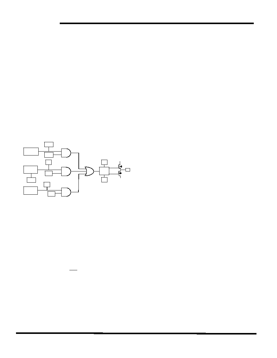
INTERRUPTS
The STK17TA8 provides three potential interrupt
sources. They include the watchdog timer, the power
monitor, and the clock/calendar alarm. Each can be
individually enabled and assigned to drive the INT pin.
In addition, each has an associated flag bit that the
host processor can use to determine the cause of the
interrupt.
Some of the sources have additional control bits that
determine functional behavior. In addition, the pin
driver has three bits that specify its behavior when an
interrupt occurs. A functional diagram of the interrupt
logic is shown below.
The three interrupts each have a source and an
enable. Both the source and the enable must be
active (true high) in order to generate an interrupt
output. Only one source is necessary to drive the pin.
The user can identify the source by reading the
Flags/Control register, which contains the flags
associated with each source. All flags are cleared to 0
when the register is read. The cycle must be a
complete read cycle ( WE high); otherwise the flags
will not be cleared. The power monitor has two pro-
grammable settings that are explained in the power
monitor section.
Once an interrupt source is active, the pin driver
determines the behavior of the output. It has two
programmable settings as shown below. Pin driver
control bits are located in the Interrupts register.
According to the programming selections, the pin can
be driven in the backup mode for an alarm interrupt.
In addition, the pin can be an active low (open-drain)
or an active high (push-pull) driver. If programmed for
operation during backup mode, it can only be active
low. Lastly, the pin can provide a one-shot function so
that the active condition is a pulse or a level condition.
In one-shot mode, the pulse width is internally fixed at
approximately 200 ms. This mode is intended to reset
a host microcontroller. In level mode, the pin goes to
its active polarity until the Flags/Control register is
read by the user. This mode is intended to be used as
an interrupt to a host microcontroller. The control bits
are summarized as follows:
Watchdog Interrupt Enable - WIE. When set to 1, the
watchdog timer drives the INT pin as well as an
internal flag when a watchdog time-out occurs. When
WIE is set to 0, the watchdog timer affects only the
internal flag.
Alarm Interrupt Enable - AIE. When set to 1, the alarm
match drives the INT pin as well as an internal flag.
When set to 0, the alarm match only affects to internal
flag.
Power Fail Interrupt Enable - PFE. When set to 1, the
power fail monitor drives the pin as well as an internal
flag. When set to 0, the power fail monitor affects only
the internal flag.
High/Low - H/L. When set to a 1, the INT pin is active
high and the driver mode is push-pull. The INT pin
can drive high only when VCC>Vswitch. When set to a 0,
the INT pin is active low and the drive mode is open-
drain. Active low (open drain) is operational even in
battery backup mode.
Pulse/Level - P/L. When set to a 1 and an interrupt
occurs, the INT pin is driven for approximately 200
ms. When P/L is set to a 0, the INT pin is driven high
or low (determined by H/L) until the Flags/Control
register is read.
When an enabled interrupt source activates the INT
pin, an external host can read the Flags/Control reg-
ister to determine the cause. Remember that all flags
will be cleared when the register is read. If the INT pin
is programmed for Level mode, then the condition will
clear and the INT pin will return to its inactive state. If
the pin is programmed for Pulse mode, then reading
the flag also will clear the flag and the pin. The pulse
will not complete its specified duration if the
Flags/Control register is read. If the INT pin is used as
a host reset, then the Flags/Control register should
not be read during a reset.
Figure 8. Interrupt Block Diagram
Watchdog
Timer
Power
Monitor
Clock
Alarm
PF
PFE
VINT
AIE
AF
P/L
H/L
Pin
Driver
INT
VCC
WIE
WDF
VSS
相关PDF资料 |
PDF描述 |
|---|---|
| STK17TA8-R25 | REAL TIME CLOCK, PDSO48 |
| STK17TA8RF25I | REAL TIME CLOCK, PDSO48 |
| STLED316SMTR | 4 X 17 SEGMENTS SEGMENT LED DRVR AND DSPL CTLR, PDSO24 |
| STM32F101C8T6 | 32-BIT, FLASH, 36 MHz, RISC MICROCONTROLLER, PQFP48 |
| STM32F101R6T6 | 32-BIT, FLASH, 36 MHz, RISC MICROCONTROLLER, PQFP64 |
相关代理商/技术参数 |
参数描述 |
|---|---|
| STK17TA8-RF25 | 功能描述:NVRAM 128Kbx8+RTC 2.7-3.6V RoHS:否 制造商:Maxim Integrated 数据总线宽度:8 bit 存储容量:1024 Kbit 组织:128 K x 8 接口类型:Parallel 访问时间:70 ns 电源电压-最大:5.5 V 电源电压-最小:4.5 V 工作电流:85 mA 最大工作温度:+ 70 C 最小工作温度:0 C 封装 / 箱体:EDIP 封装:Tube |
| STK17TA8-RF25I | 功能描述:NVRAM 128Kbx8+RTC 2.7-3.6V RoHS:否 制造商:Maxim Integrated 数据总线宽度:8 bit 存储容量:1024 Kbit 组织:128 K x 8 接口类型:Parallel 访问时间:70 ns 电源电压-最大:5.5 V 电源电压-最小:4.5 V 工作电流:85 mA 最大工作温度:+ 70 C 最小工作温度:0 C 封装 / 箱体:EDIP 封装:Tube |
| STK17TA8-RF25IL | 制造商:Cypress Semiconductor 功能描述: |
| STK17TA8-RF25ITR | 功能描述:NVRAM 128Kbx8+RTC 2.7-3.6V RoHS:否 制造商:Maxim Integrated 数据总线宽度:8 bit 存储容量:1024 Kbit 组织:128 K x 8 接口类型:Parallel 访问时间:70 ns 电源电压-最大:5.5 V 电源电压-最小:4.5 V 工作电流:85 mA 最大工作温度:+ 70 C 最小工作温度:0 C 封装 / 箱体:EDIP 封装:Tube |
| STK17TA8-RF25TR | 功能描述:NVRAM 128Kbx8+RTC 2.7-3.6V RoHS:否 制造商:Maxim Integrated 数据总线宽度:8 bit 存储容量:1024 Kbit 组织:128 K x 8 接口类型:Parallel 访问时间:70 ns 电源电压-最大:5.5 V 电源电压-最小:4.5 V 工作电流:85 mA 最大工作温度:+ 70 C 最小工作温度:0 C 封装 / 箱体:EDIP 封装:Tube |
发布紧急采购,3分钟左右您将得到回复。