参数资料
| 型号: | SY10EP16VKC |
| 厂商: | Micrel Inc |
| 文件页数: | 4/6页 |
| 文件大小: | 0K |
| 描述: | IC RCVR HS DIFF 5V/3.3V 8-MSOP |
| 标准包装: | 100 |
| 系列: | 10EP |
| 逻辑类型: | 差分接收器/驱动器 |
| 电源电压: | 3 V ~ 5.5 V |
| 工作温度: | -40°C ~ 85°C |
| 安装类型: | 表面贴装 |
| 封装/外壳: | 8-TSSOP,8-MSOP(0.118",3.00mm 宽) |
| 供应商设备封装: | 8-MSOP |
| 包装: | 管件 |
Micrel, Inc.
SY89202U
August 2007
4
M9999-083107-C
hbwhelp@micrel.com or (408) 955-1690
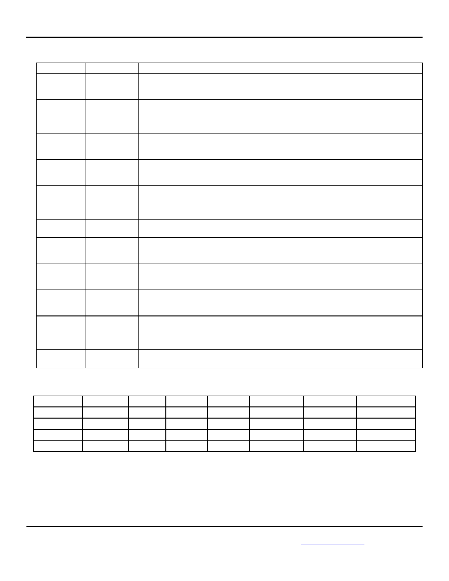
Pin Description
Pin Number
Pin Name
Pin Function
2, 7, 8
DIVSEL1
DIVSEL2
DIVSEL3
Single-Ended Inputs: These TTL/CMOS inputs select the divide ratio for each of the three
banks of outputs. Note that each of these inputs is internally connected to a 25k
pull-up
resistor and will default to logic HIGH state if left open. The input-switching threshold is VCC/2.
3, 6
IN, /IN
Differential Input: This input pair is the differential signal input to the device. This input accepts
AC- or DC-coupled signals as small as 100mV. The input pair internally terminates to a VT pin
through 50
. Note that these inputs will default to an indeterminate state if left open. Please
refer to the “Input Interface Applications” section for more details.
4
VT
Input Termination Center-Tap: Each side of the differential input pair terminates to the VT pin.
The VT pin provides a center-tap to a termination network for maximum interface flexibility.
See “Input Interface Applications” section for more details.
5
VREF-AC
Reference Voltage: This output biases to VCC –1.2V. It is used for AC-coupling inputs IN and
/IN. For AC-coupled applications, connect VREF-AC directly to the VT pin. Bypass with 0.01F
low ESR capacitor to VCC.
9
EN
Single-Ended Input: This TTL/CMOS input disables and enables the Q0 – Q7 outputs. This
input is internally connected to a 25k
pull-up resistor and will default to logic HIGH state if left
open. The input-switching threshold is VCC/2. For the input enable and disable functional
description, refer to “Timing Diagram” section.
10, 19, 22, 31
VCC
Positive power supply. Bypass with 0.1F||0.01F low ESR capacitors as close to VCC pins
as possible.
16, 15, 14,
13, 12, 11
Q4, /Q4, Q5,
/Q5, Q6, /Q6
Bank 2 LVPECL differential output pairs controlled by DIVSEL2: LOW, Q4 – Q6 = ÷2, HIGH,
Q4 – Q6 = ÷4. Unused output pairs may be left open. Each output is designed to drive 800mV
into 50
terminated at VCC–2V.
30, 29, 28,
27, 26, 25,
24, 23
Q0, /Q0, Q1,
/Q1, Q2, /Q2,
Q3, /Q3
Bank 1 LVPECL differential output pairs controlled by DIVSEL1: LOW, Q0 – Q3 = ÷1, HIGH,
Q0 – Q3 = ÷2. Unused output pairs may be left open. Each output is designed to drive 800mV
into 50
terminated at VCC–2V.
18, 17
Q7, /Q7
Bank 3 LVPECL differential output pair controlled by DIVSEL3: LOW, Q7 = ÷2, HIGH, Q7 =
÷4. Unused output pairs may be left open. Each output is designed to drive 800mV into 50
terminated at VCC–2V.
32
/MR
Single-Ended Input: This TTL/CMOS-compatible master reset function asynchronously sets
Q0 – Q7 outputs LOW and /Q0 – /Q7 outputs HIGH, and holds them in that state as long as
the /MR input remains LOW. This input is internally connected to a 25k
pull-up resistor and
will default to a logic HIGH state if left open. The input-switching threshold is VCC/2.
1, 20, 21
GND,
Exposed Pad
Ground: Ground pin and exposed pad must be connected to the same ground plane.
Truth Table
/MR
( 1)
EN
( 2, 3)
DIVSEL1
DIVSEL2
DIVSEL3
Q0 – Q3
Q4 – Q6
Q7
0
X
0
1
0
X
0
1
0
1
2
1
2
4
Notes:
1. /MR asynchronously forces Q0 – Q7 LOW (/Q0 - /Q7 HIGH).
2. EN forces Q0 – Q7 LOW between 2 and 6 input clock cycles after the falling edge of EN. Refer to “Timing Diagram” section.
3. EN synchronously enables the outputs between 2 and 6 input clock cycles after the rising edge of EN. Refer to “Timing Diagram” section.
相关PDF资料 |
PDF描述 |
|---|---|
| VE-B5M-IV-B1 | CONVERTER MOD DC/DC 10V 150W |
| VE-B51-IV-B1 | CONVERTER MOD DC/DC 12V 150W |
| VE-B50-IV-B1 | CONVERTER MOD DC/DC 5V 150W |
| VE-B4D-MW-F3 | CONVERTER MOD DC/DC 85V 100W |
| MS3451W10SL-3P | CONN RCPT 3POS CBL MNT W/PINS |
相关代理商/技术参数 |
参数描述 |
|---|---|
| SY10EP16VKC TR | 功能描述:IC RCVR HS DIFF 5V/3.3V 8-MSOP RoHS:否 类别:集成电路 (IC) >> 逻辑 - 专用逻辑 系列:10EP 产品变化通告:Product Discontinuation 25/Apr/2012 标准包装:1,500 系列:74SSTV 逻辑类型:DDR 的寄存缓冲器 电源电压:2.3 V ~ 2.7 V 位数:14 工作温度:0°C ~ 70°C 安装类型:表面贴装 封装/外壳:48-TFSOP(0.240",6.10mm 宽) 供应商设备封装:48-TSSOP 包装:带卷 (TR) |
| SY10EP16VKG | 功能描述:缓冲器和线路驱动器 3.3V/5V Differential Receiver (I Temp, Green) RoHS:否 制造商:Micrel 输入线路数量:1 输出线路数量:2 极性:Non-Inverting 电源电压-最大:+/- 5.5 V 电源电压-最小:+/- 2.37 V 最大工作温度:+ 85 C 安装风格:SMD/SMT 封装 / 箱体:MSOP-8 封装:Reel |
| SY10EP16VKG TR | 功能描述:缓冲器和线路驱动器 3.3V/5V Differential Receiver (I Temp, Green) RoHS:否 制造商:Micrel 输入线路数量:1 输出线路数量:2 极性:Non-Inverting 电源电压-最大:+/- 5.5 V 电源电压-最小:+/- 2.37 V 最大工作温度:+ 85 C 安装风格:SMD/SMT 封装 / 箱体:MSOP-8 封装:Reel |
| SY10EP16VKI | 功能描述:IC RCVR HS DIFF 5V/3.3V 8-MSOP RoHS:否 类别:集成电路 (IC) >> 逻辑 - 专用逻辑 系列:10EP 产品变化通告:Product Discontinuation 25/Apr/2012 标准包装:1,500 系列:74SSTV 逻辑类型:DDR 的寄存缓冲器 电源电压:2.3 V ~ 2.7 V 位数:14 工作温度:0°C ~ 70°C 安装类型:表面贴装 封装/外壳:48-TFSOP(0.240",6.10mm 宽) 供应商设备封装:48-TSSOP 包装:带卷 (TR) |
| SY10EP16VKI TR | 功能描述:IC RCVR HS DIFF 5V/3.3V 8-MSOP RoHS:否 类别:集成电路 (IC) >> 逻辑 - 专用逻辑 系列:10EP 产品变化通告:Product Discontinuation 25/Apr/2012 标准包装:1,500 系列:74SSTV 逻辑类型:DDR 的寄存缓冲器 电源电压:2.3 V ~ 2.7 V 位数:14 工作温度:0°C ~ 70°C 安装类型:表面贴装 封装/外壳:48-TFSOP(0.240",6.10mm 宽) 供应商设备封装:48-TSSOP 包装:带卷 (TR) |
发布紧急采购,3分钟左右您将得到回复。