参数资料
| 型号: | SY58600UMI TR |
| 厂商: | Micrel Inc |
| 文件页数: | 4/10页 |
| 文件大小: | 0K |
| 描述: | IC LINEDRIVER/RCVR CML DIFF 8MLF |
| 标准包装: | 1,000 |
| 系列: | SY58 |
| 逻辑类型: | 差分接收器/驱动器 |
| 电源电压: | 3 V ~ 3.6 V |
| 工作温度: | -40°C ~ 85°C |
| 安装类型: | 表面贴装 |
| 封装/外壳: | 8-VFDFN 裸露焊盘,8-MLF? |
| 供应商设备封装: | 8-MLF?(2x2) |
| 包装: | 带卷 (TR) |
| 其它名称: | 576-1536-2 SY58600UMI TR-ND SY58600UMITR |
3
Precision Edge
SY58600U
Micrel, Inc.
M9999-082707
hbwhelp@micrel.com or (408) 955-1690
Absolute Maximum Ratings(1)
Supply Voltage (V
CC) .................................. –0.5V to +4.0V
Input Voltage (V
IN) ......................................... –0.5V to VCC
CML Output Voltage (V
OUT) ......... VCC –1.0V to VCC +0.5V
Termination Current(3)
Source or Sink Current on V
T .................................... ±100mA
Input Current
Source or Sink Current on IN, /IN ........................ ±50mA
Current (V
REF)
Source or Sink Current on V
REF–AC .................. ±1.5mA
Lead Temperature (soldering, 20 sec.) ................... +260°C
Storage Temperature (T
S) ....................... –65°C to +150°C
Operating Ratings(2)
Supply Voltage (V
CC) ...................... +2.375V to +2.625V or
............................................................ +3.0V to +3.6V
Ambient Temperature (T
A) ......................... –40°C to +85°C
Package Thermal Resistance(4)
MLF (θJA)
Still-Air ............................................................. 93°C/W
MLF (ψJB)
Junction-to-Board ............................................ 32°C/W
T
A = –40°C to +85°C, unless otherwise noted.
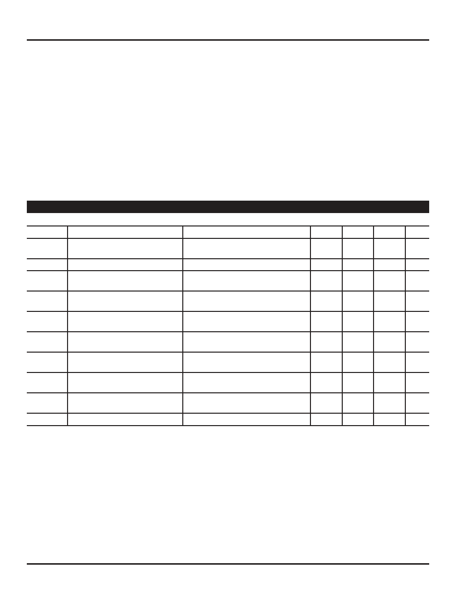
Symbol
Parameter
Condition
Min
Typ
Max
Units
V
CC
Power Supply
V
CC = 2.5V
2.375
2.5
2.625
V
CC = 3.3V
3.0
3.3
3.6
V
I
CC
Power Supply Current
No Load, max. V
CC, Note 6
45
65
mA
R
DIFF_IN
Differential Input Resistance
80
100
120
(IN-to-/IN)
R
IN
Input Resistance
40
50
60
(IN-to-V
T, /IN-to-VT)
V
IH
Input HIGH Voltage
Note 7
V
CC –1.6
V
CC
V
(IN, /IN)
V
IL
Input LOW Voltage
0
V
IH –0.1
V
(IN, /IN)
V
IN
Input Voltage Swing
See Figure 1a.
0.1
1.7
V
(IN, /IN)
V
DIFF_IN
Differential Input Voltage Swing
See Figure 1b.
0.2
V
|IN–, /IN|
V
T_IN
In-to-V
T
1.28
V
(IN, /IN)
V
REF–AC
Output Reference Voltage
V
CC –1.3 VCC –1.2 VCC –1.1
V
Notes:
1. Permanent device damage may occur if the ratings in “Absolute Maximum Ratings” section are exceeded. This is a stress rating only and functional
operation is not implied for conditions other than those detailed in the operational sections of this data sheet. Exposure to absolute maximum ratings
conditions for extended periods may affect device reliability.
2. The data sheet limits are not guaranteed if the device is operated beyond the operating ratings.
3. Due to the limited drive capability use for input of the same package only.
4. Package thermal resistance assumes exposed pad is soldered (or equivalent) to the device’s most negative potential on the PCB. ψJB uses 4-layer
θJA in still-air, unless otherwise stated.
5. The circuit is designed to meet the DC specifications shown in the above table after thermal equilibrium has been established.
6. Includes current through internal 50 pull-ups.
7. V
IH (min) not lower than 1.2V.
DC ELECTRICAL CHARACTERISTICS(5)
相关PDF资料 |
PDF描述 |
|---|---|
| AT42QT1010-MAH | IC SENSR TOUCH/PROX 1CH 8UDFN |
| VE-JWR-MX-F1 | CONVERTER MOD DC/DC 7.5V 75W |
| MS27467T11F98PB | CONN PLUG 6POS STRAIGHT W/PINS |
| MS27467T15B18PC | CONN PLUG 18POS STRAIGHT W/PINS |
| VE-JWP-MX-F4 | CONVERTER MOD DC/DC 13.8V 75W |
相关代理商/技术参数 |
参数描述 |
|---|---|
| SY58601U | 制造商:MICREL 制造商全称:Micrel Semiconductor 功能描述:ULTRA-PRECISION DIFFERENTIAL CML LINE DRIVER/RECEIVER WITH INTERNAL TERMINATION |
| SY58601UMG TR | 功能描述:缓冲器和线路驱动器 Ultra-small, ultra-low jitter LVPECL Buffer (I Temp, Green) RoHS:否 制造商:Micrel 输入线路数量:1 输出线路数量:2 极性:Non-Inverting 电源电压-最大:+/- 5.5 V 电源电压-最小:+/- 2.37 V 最大工作温度:+ 85 C 安装风格:SMD/SMT 封装 / 箱体:MSOP-8 封装:Reel |
| SY58601UMGTR | 制造商:Micrel 功能描述:Differential Line Receiver 800mV Single |
| SY58601UMG-TR | 功能描述:IC LDRVR/RCVR LVPECL 800MV 8MLF 制造商:microchip technology 系列:SY58 包装:剪切带(CT) 零件状态:有效 逻辑类型:差分接收器/驱动器 电源电压:2.375 V ~ 2.625 V,3 V ~ 3.6 V 位数:1 工作温度:-40°C ~ 85°C 安装类型:表面贴装 封装/外壳:8-VFDFN 裸露焊盘,8-MLF? 供应商器件封装:8-MLF?(2x2) 标准包装:1 |
| SY58601UMI | 制造商:Micrel Inc 功能描述: |
发布紧急采购,3分钟左右您将得到回复。