参数资料
| 型号: | SY89474UMG |
| 厂商: | Micrel Inc |
| 文件页数: | 5/11页 |
| 文件大小: | 0K |
| 描述: | IC MUX 2:1 LVDS 1:2 FANOUT 24MLF |
| 标准包装: | 75 |
| 系列: | SY89 |
| 类型: | 多路复用器 |
| 电路: | 1 x 2:1 |
| 独立电路: | 1 |
| 电压电源: | 单电源 |
| 电源电压: | 3 V ~ 3.6 V |
| 工作温度: | -40°C ~ 85°C |
| 安装类型: | 表面贴装 |
| 封装/外壳: | 24-VFQFN 裸露焊盘,24-MLF? |
| 供应商设备封装: | 24-MLF?(4x4) |
| 包装: | 管件 |
| 产品目录页面: | 1090 (CN2011-ZH PDF) |
| 其它名称: | 576-2562 SY89474UMG-ND |
Micrel, Inc.
SY89474U
August 2005
3
M9999-081105
hbwhelp@micrel.com or (408) 955-1690
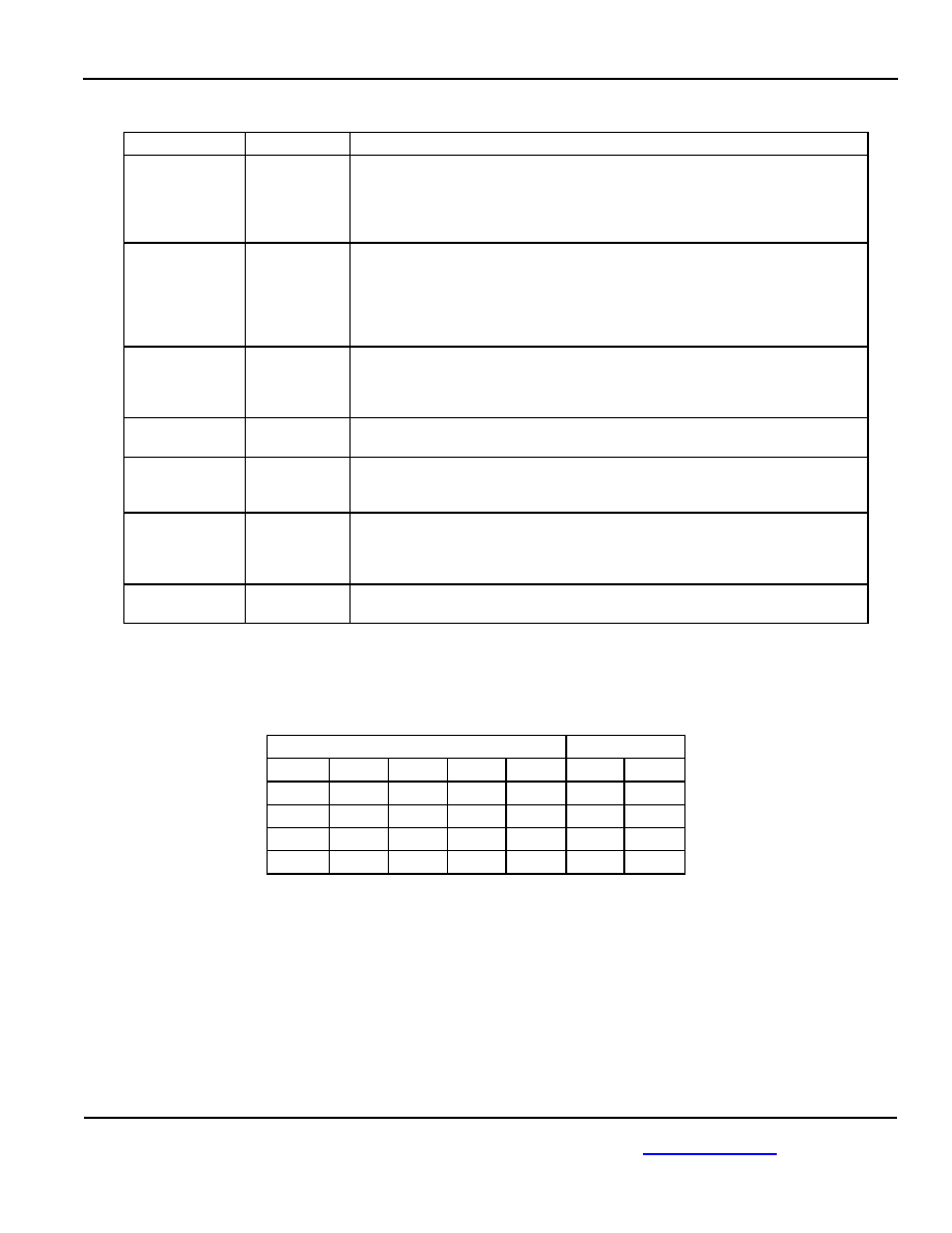
Pin Description
Pin Number
Pin Name
Pin Function
5, 2,
23, 20
IN0, /IN0
IN1, /IN1
Differential Inputs: These input pairs are the differential signal inputs to the
device. They accept AC- or DC-coupled signals as small as 100mV (200mVpp).
Note that these inputs will default to an undetermined state if left open. Each pin
of a pair internally terminates to a VT pin through 50. Please refer to the “Input
Interface Applications” section for more details.
3, 21
VREF-AC0,
VREF-AC1
Reference Voltage: These outputs bias to VCC -1.2V. They are used for AC-
coupling inputs IN and /IN. Connect VREF-AC directly to the corresponding VT
pin. Bypass with 0.01F low ESR capacitor to VCC. Maximum sink/source
current is ±1.5mA. Due to the limited drive capability, the VREF-AC pin is only
intended to drive its respective VT pin. Please refer to the “Input Interface
Applications” section for more details.
4, 22
VT0, VT1
Input Termination Center-Tap: Each side of the differential input pair terminates
to a VT pin. The VT0 and VT1 pins provide a center-tap to a termination network
for maximum interface flexibility. Please refer to the “Input Interface Applications”
section for more details.
1, 6, 9, 10, 13,
19, 24
VCC
Positive Power Supply: Connect to +2.5V ±5% power supply. Bypass with
0.1F//0.01F low ESR capacitors as close to VCC pins as possible.
7, 8
11, 12
Q0, /Q0
Q1, /Q1
Differential Outputs: These differential LVDS output pairs are a logic function of
the IN0, IN1, and SEL inputs. Please refer to the truth table below for details.
Unused output pairs should be terminated with 100 across the outputs.
15
SEL
This single-ended TTL/CMOS-compatible input selects the inputs to the
multiplexer. Note that this input is internally connected to a 25k pull-up resistor
and will default to a logic HIGH state if left open. VTH = VCC/2. Please refer to the
“Timing Diagram” section for more details.
14, 17, 18
GND,
Exposed Pad
Ground: Ground pins and exposed pad must be connected to the same ground
plane.
Truth Table
INPUTS
OUTPUTS
IN0
/IN0
IN1
/IN1
SEL
Q
/Q
0
1
X
0
1
0
X
0
1
0
X
0
1
0
1
X
1
0
1
0
相关PDF资料 |
PDF描述 |
|---|---|
| VI-J10-MX-F1 | CONVERTER MOD DC/DC 5V 75W |
| VI-J0P-MX-F2 | CONVERTER MOD DC/DC 13.8V 75W |
| MS27656T25F43SB | CONN RCPT 43POS WALL MNT W/SCKT |
| D38999/20SE99PN | CONN RCPT 23POS WALL MNT W/PINS |
| MS3450L18-4PZ | CONN RCPT 4POS WALL MNT W/PINS |
相关代理商/技术参数 |
参数描述 |
|---|---|
| SY89474UMG TR | 功能描述:编码器、解码器、复用器和解复用器 2.5/3.3V 2:1 LVDS MUX w/ 1:2 Fanout (I Temp, Green) RoHS:否 制造商:Micrel 产品:Multiplexers 逻辑系列:CMOS 位数: 线路数量(输入/输出):2 / 12 传播延迟时间:350 ps, 400 ps 电源电压-最大:2.625 V, 3.6 V 电源电压-最小:2.375 V, 3 V 最大工作温度:+ 85 C 安装风格:SMD/SMT 封装 / 箱体:QFN-44 封装:Tray |
| SY89474UMGTR | 制造商:MICREL 制造商全称:Micrel Semiconductor 功能描述:Precision LVDS 2:1 Multiplexer with 1:2 |
| SY89475U | 制造商:MICREL 制造商全称:Micrel Semiconductor 功能描述:Precision LVPECL 2:1 Multiplexer with 1:2 Fanout and Internal Termination |
| SY89529L | 制造商:MICREL 制造商全称:Micrel Semiconductor 功能描述:3.3V 200MHz PRECISION SPREADSPECTRUM CLOCK SYNTHESIZER |
| SY89529LTC | 功能描述:IC SYNTHESIZER CLK 200MHZ 32TQFP RoHS:否 类别:集成电路 (IC) >> 时钟/计时 - 时钟发生器,PLL,频率合成器 系列:Precision Edge® 产品变化通告:Product Discontinuation 04/May/2011 标准包装:96 系列:- 类型:时钟倍频器,零延迟缓冲器 PLL:带旁路 输入:LVTTL 输出:LVTTL 电路数:1 比率 - 输入:输出:1:8 差分 - 输入:输出:无/无 频率 - 最大:133.3MHz 除法器/乘法器:是/无 电源电压:3 V ~ 3.6 V 工作温度:0°C ~ 70°C 安装类型:表面贴装 封装/外壳:16-TSSOP(0.173",4.40mm 宽) 供应商设备封装:16-TSSOP 包装:管件 其它名称:23S08-5HPGG |
发布紧急采购,3分钟左右您将得到回复。