参数资料
| 型号: | SY89826LHY |
| 厂商: | Micrel Inc |
| 文件页数: | 6/10页 |
| 文件大小: | 0K |
| 描述: | IC CLK BUF MUX TRNSL 2:22 64TQFP |
| 标准包装: | 160 |
| 系列: | Precision Edge® |
| 类型: | 扇出缓冲器(分配),多路复用器,变换器 |
| 电路数: | 1 |
| 比率 - 输入:输出: | 2:22 |
| 差分 - 输入:输出: | 是/是 |
| 输入: | LVDS,LVPECL |
| 输出: | LVDS |
| 频率 - 最大: | 1GHz |
| 电源电压: | 3 V ~ 3.6 V |
| 工作温度: | -40°C ~ 85°C |
| 安装类型: | 表面贴装 |
| 封装/外壳: | 64-TQFP 裸露焊盘 |
| 供应商设备封装: | 64-EP-TQFP |
| 包装: | 托盘 |
| 产品目录页面: | 1090 (CN2011-ZH PDF) |
| 其它名称: | 576-2567 SY89826LHY-ND |
5
Precision Edge
SY89826L
Micrel, Inc.
M9999-011907
hbwhelp@micrel.com or (408) 955-1690
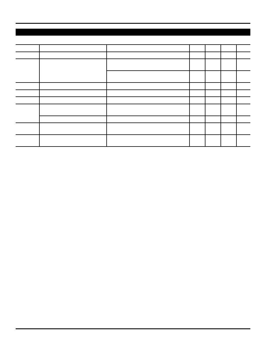
VCC = 3.3V ±10%, TA = –40°C to +85°C, unless noted.
Symbol
Parameter
Condition
Min
Typ
Max
Units
fMAX
Maximum Toggle Frequency
Note 2
1.0
GHz
tPHL
Differential Propagation Delay,
LVPECL Input: 150mV
0.750
1.0
1.250
ns
tPLH
Note 3
LVPECL Input: 800mV
0.6
0.850
1.10
ns
LVDS Input: 100mV
0.950
1.2
1.450
ns
LVDS Input: 400mV
0.800
1.0
1.30
ns
tSWITCHOVER Clock Input Switchover
CLK_SEL-to-Valid Output
1.4
1.7
ns
tS(OE)
Output Enable Set-Up Time
Note 4
1.0
ns
tH(OE)
Output Enable Hold Time
Note 4
0.5
ns
tskew
Within Device Skew
Note 5
0
°C to +85°C25
50
ps
–40
°C75
ps
Part-to-Part Skew
Note 6
400
ps
tJITTER
Cycle-to-Cycle
Note 7
1ps
RMS
Total Jitter
Note 8
<1
2
ps
PP
tr, tf
Output Rise/Fall Times
200
290
400
ps
(20% to 80%)
Note 1.
100
termination between Q and /Q outputs. Airflow ≥300lfpm, or exposed pad soldered to ground plane. Typicals are at nominal supply,
T
A = 25°C.
Note 2.
fMAX is defined as the maximum toggle frequency, measured with a 750mV LVPECL input or 350mV LVDS input. Output swing is ≥ 200mV.
Note 3.
Differential propagation delay is defined as the delay from the crossing point of the differential input signals to the crossing point of the differential
output signals.
Note 4.
Set-up and hold time applies to synchronous applications that intend to enable/disable before the next clock cycle. For asynchronous applications,
set-up and hold time does not apply. OE set-up time is defined with respect to the rising edge of the clock. OE HIGH to LOW transition ensures
outputs remain disabled during the next clock cycle. OE LOW to HIGH transition enables normal operation of the next input clock.
Note 5.
The within-device skew is defined as the worst case difference between any two similar delay paths within a single device with identical input
transition, operating at the same voltage and temperature.
Note 6.
The part-to-part skew is defined as the absolute worst case difference between any two delay paths on any two devices operating at the same voltage
and temperature. Part-to-part skew is the total skew difference; pin-to-pin skew + part-to-part skew.
Note 7.
Cycle-to-cycle jitter definition: The variation in period between adjacent cycles over a random sample of adjacent cycle pairs. T
JITTER_CC =Tn–Tn+1
where T is the time between rising edges of the output signal.
Note 8.
Total jitter definition: with an ideal clock input, no more than one output edge in 1012 output edges will deviate by more than the specified peak-to-
peak jitter value.
AC ELECTRICAL CHARACTERISTICS(1)
相关PDF资料 |
PDF描述 |
|---|---|
| LTC6993MPS6-4#TRPBF | IC MULTIVIBRATOR MONO TSOT23-6 |
| LTC6993MPS6-4#TRMPBF | IC MULTIVIBRATOR MONO TSOT23-6 |
| D38999/24MJ8BN | CONN HSG RCPT 8POS JAM NUT SCKT |
| VI-BWT-MX | CONVERTER MOD DC/DC 6.5V 75W |
| D38999/26MJ8BE | CONN HSG PLUG 8POS STRGHT SCKT |
相关代理商/技术参数 |
参数描述 |
|---|---|
| SY89826LHY TR | 功能描述:时钟合成器/抖动清除器 3.3V 1:22 LVDS Fanout/Translator (I Temp, Lead Free) RoHS:否 制造商:Skyworks Solutions, Inc. 输出端数量: 输出电平: 最大输出频率: 输入电平: 最大输入频率:6.1 GHz 电源电压-最大:3.3 V 电源电压-最小:2.7 V 封装 / 箱体:TSSOP-28 封装:Reel |
| SY89826LHYTR | 制造商:MICREL 制造商全称:Micrel Semiconductor 功能描述:3.3V 1GHz PRECISION 1:22 LVDS FANOUT BUFFER/TRANSLATOR WITH 2:1 INPUT MUX |
| SY89827L | 制造商:MICREL 制造商全称:Micrel Semiconductor 功能描述:3.3V 500MHz DUAL 1:10 HSTL FANOUT BUFFER/TRANSLATOR WITH 2:1 MUX INPUT |
| SY89827L_10 | 制造商:MICREL 制造商全称:Micrel Semiconductor 功能描述:3.3V 500MHz DUAL 1:10 HSTL FANOUT BUFFER/TRANSLATOR WITH 2:1 MUX INPUT |
| SY89827LHG | 制造商:Micrel Inc 功能描述:IC, FANOUT BUFFER/TRANSLATOR, TQFP-64, Logic Device Type:Buffer, Translator, Sup |
发布紧急采购,3分钟左右您将得到回复。