- 您现在的位置:买卖IC网 > PDF目录98150 > SY89827LHGTR (MICREL INC) 89827 SERIES, LOW SKEW CLOCK DRIVER, 20 TRUE OUTPUT(S), 0 INVERTED OUTPUT(S), PQFP64 PDF资料下载
参数资料
| 型号: | SY89827LHGTR |
| 厂商: | MICREL INC |
| 元件分类: | 时钟及定时 |
| 英文描述: | 89827 SERIES, LOW SKEW CLOCK DRIVER, 20 TRUE OUTPUT(S), 0 INVERTED OUTPUT(S), PQFP64 |
| 封装: | LEAD FREE, TQFP-64 |
| 文件页数: | 9/11页 |
| 文件大小: | 747K |
| 代理商: | SY89827LHGTR |
7
Precision Edge
SY89827L
Micrel, Inc.
M9999-061306
hbwhelp@micrel.com or (408) 955-1690
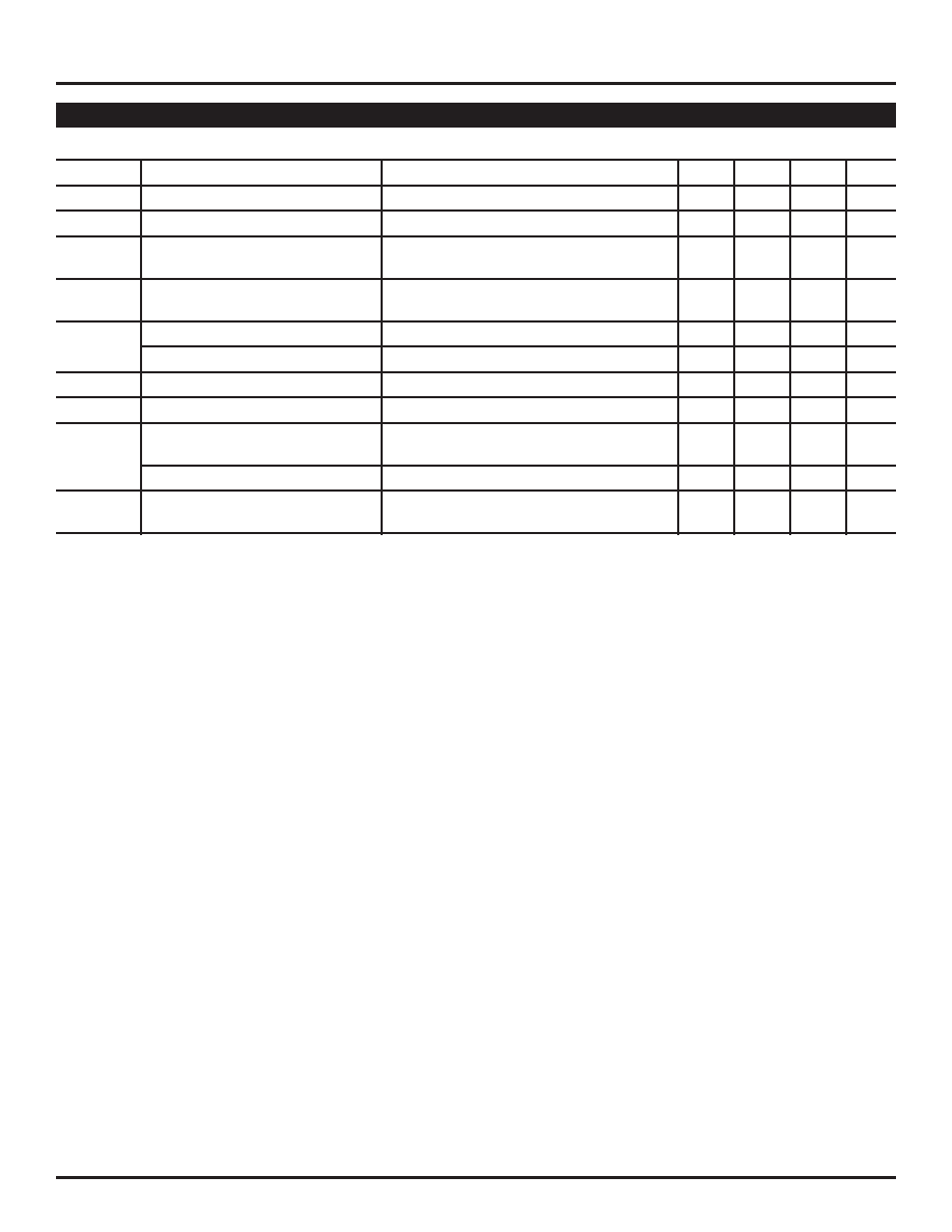
VCCI = 3.3V ±5%, VCCO = 1.8V ±10%, TA = –40°C to +85°C, all outputs loaded, unless noted.
Symbol
Parameter
Condition
Min
Typ
Max
Units
fMAX
Maximum Toggle Frequency
Note 2
500
MHz
tPD
Differential Propagation Delay
Note 3
1.0
1.3
1.5
ns
VPP
Minimum Input Swing, Note 4
HSTL
200
mV
PECL
150
mV
t
SW
Switchover Time
CLK_SEL-to-Q
1.6
2.0
ns
SEL-to-Q
1.4
1.75
ns
tJITTER
Cycle-to-Cycle
Note 8
<1
ps
RMS
Total Jitter
Note 9
<10
ps
PP
tS(OE)
Output Enable Set-Up Time
Note 5
1.0
ns
tH(OE)
Output Enable Hold Time
Note 5
0.5
ns
tskew
Within Device Skew
Note 6
0°C to +85°C25
50
ps
–40°C35
75
ps
Part-to-Part Skew
Note 7
400
ps
tr, tf
Output Rise/Fall Times
450
700
ps
(20% to 80%)
Note 1.
Outputs loaded with 50-t- ground.
Note 2.
fMAX is defined as the maximum toggle frequency, measured with a 750mV LVPECL/HSTL input. HSTL output swing is > 400mV.
Note 3.
Differential propagation delay is defined as the delay from the crossing point of the differential input signals to the crossing point of the differential
output signals.
Note 4.
The VPP (min.) is defined as the minimum input differential voltage which will cause no increase in the propagation delay.
Note 5.
OE set-up time is defined with respect to the rising edge of the clock. OE HIGH-to-LOW transition ensures outputs remain disabled during the next
clock cycle. OE LOW-to-HIGH transition enables normal operation of the next input clock.
Note 6.
The within-device skew is defined as the worst case difference between any two similar delay paths within a single device operating at the same
voltage and temperature. This parameters includes within bank skew and bank-to-bank skew.
Note 7.
The part-to-part skew is defined as the absolute worst case difference between any two delay paths on any two devices operating at the same voltage
and temperature.
Note 8.
Cycle-to-cycle jitter definition: The variation in period between adjacent cycles over a random sample of adjacent cycle pairs. TJITTER_CC =Tn–Tn+1
where T is the time between rising edges of the output signal.
Note 9.
Total jitter definition: with an ideal clock input, no more than one output edge in 1012 output edges will deviate by more than the specified peak-
to-peak jitter value.
AC ELECTRICAL CHARACTERISTICS(NOTE 1)
相关PDF资料 |
PDF描述 |
|---|---|
| SY89833ALMGTR | 89833 SERIES, LOW SKEW CLOCK DRIVER, 4 TRUE OUTPUT(S), 0 INVERTED OUTPUT(S), QCC16 |
| SY89833ALMI | 89833 SERIES, LOW SKEW CLOCK DRIVER, 4 TRUE OUTPUT(S), 0 INVERTED OUTPUT(S), QCC16 |
| SY89833ALMITR | 89833 SERIES, LOW SKEW CLOCK DRIVER, 4 TRUE OUTPUT(S), 0 INVERTED OUTPUT(S), QCC16 |
| SY89837UMTR | 89837 SERIES, LOW SKEW CLOCK DRIVER, 8 TRUE OUTPUT(S), 0 INVERTED OUTPUT(S), QCC32 |
| SY89837UMY | 89837 SERIES, LOW SKEW CLOCK DRIVER, 8 TRUE OUTPUT(S), 0 INVERTED OUTPUT(S), QCC32 |
相关代理商/技术参数 |
参数描述 |
|---|---|
| SY89827LHI | 功能描述:IC CLK FANT BUF MUX TRNSL 64TQFP RoHS:否 类别:集成电路 (IC) >> 时钟/计时 - 时钟缓冲器,驱动器 系列:Precision Edge® 标准包装:1 系列:HiPerClockS™ 类型:扇出缓冲器(分配),多路复用器 电路数:1 比率 - 输入:输出:2:18 差分 - 输入:输出:是/无 输入:CML,LVCMOS,LVPECL,LVTTL,SSTL 输出:LVCMOS,LVTTL 频率 - 最大:250MHz 电源电压:2.375 V ~ 3.465 V 工作温度:0°C ~ 70°C 安装类型:表面贴装 封装/外壳:32-LQFP 供应商设备封装:32-TQFP(7x7) 包装:- 其它名称:800-1923-6 |
| SY89827LHITR | 制造商:MICREL 制造商全称:Micrel Semiconductor 功能描述:3.3V 500MHz DUAL 1:10 HSTL FANOUT BUFFER/TRANSLATOR WITH 2:1 MUX INPUT |
| SY89827LHY | 功能描述:时钟缓冲器 3.3V Dual 1:20 Diff HSTL Fanout Buffer (I Temp, Lead Free) RoHS:否 制造商:Texas Instruments 输出端数量:5 最大输入频率:40 MHz 传播延迟(最大值): 电源电压-最大:3.45 V 电源电压-最小:2.375 V 最大功率耗散: 最大工作温度:+ 85 C 最小工作温度:- 40 C 封装 / 箱体:LLP-24 封装:Reel |
| SY89827LHY TR | 功能描述:时钟缓冲器 3.3V Dual 1:20 Diff HSTL Fanout Buffer (I Temp, Lead Free) RoHS:否 制造商:Texas Instruments 输出端数量:5 最大输入频率:40 MHz 传播延迟(最大值): 电源电压-最大:3.45 V 电源电压-最小:2.375 V 最大功率耗散: 最大工作温度:+ 85 C 最小工作温度:- 40 C 封装 / 箱体:LLP-24 封装:Reel |
| SY89827LHYTR | 制造商:MICREL 制造商全称:Micrel Semiconductor 功能描述:3.3V 500MHz DUAL 1:10 HSTL FANOUT BUFFER/TRANSLATOR WITH 2:1 MUX INPUT |
发布紧急采购,3分钟左右您将得到回复。