参数资料
| 型号: | SY89843UMG TR |
| 厂商: | Micrel Inc |
| 文件页数: | 16/17页 |
| 文件大小: | 0K |
| 描述: | IC MUX CML RPE 2:1 PREC 24-MLF |
| 标准包装: | 1,000 |
| 系列: | SY89 |
| 类型: | 多路复用器 |
| 电路: | 1 x 2:1 |
| 独立电路: | 1 |
| 电压电源: | 单电源 |
| 电源电压: | 3 V ~ 3.6 V |
| 工作温度: | -40°C ~ 85°C |
| 安装类型: | 表面贴装 |
| 封装/外壳: | 24-VFQFN 裸露焊盘,24-MLF? |
| 供应商设备封装: | 24-MLF?(4x4) |
| 包装: | 带卷 (TR) |
| 其它名称: | SY89843UMGTR SY89843UMGTR-ND |
Micrel, Inc.
SY89843U
Oct. 1, 2013
8
M9999-052207-B
hbwhelp@micrel.com or (408) 955-1690
Functional Description
RPE MUX and Fail-Safe Input
The SY89843U is optimized for clock switchover
applications where switching from one clock to
another clock without runt pulses (short cycles) is
required. It features two unique circuits:
Runt-Pulse Eliminator (RPE) Circuit:
The RPE MUX provides a “glitchless” switchover
between two clocks and prevents any runt pulses
from occurring during the switchover transition. The
design of both clock inputs is identical (i.e., the
switchover sequence and protection is symmetrical
for both input pair, IN0 or IN1. Thus, either input pair
may be defined as the primary input). If not required,
the RPE function can be permanently disabled to
allow the switchover between inputs to occur
immediately. If the CAP pin is tied directly to VCC,
then the RPE function will be disabled and the
multiplexer will function as a normal multiplexer.
Fail-Safe Input (FSI) Circuit:
The FSI function provides protection against a
selected input pair that drops below the minimum
amplitude requirement. If the selected input pair
drops sufficiently below the 100mV minimum single-
ended
input
amplitude
limit
(VIN),
or
200mV
differentially (VDIFF_IN), then the output will latch to
the last valid clock state.
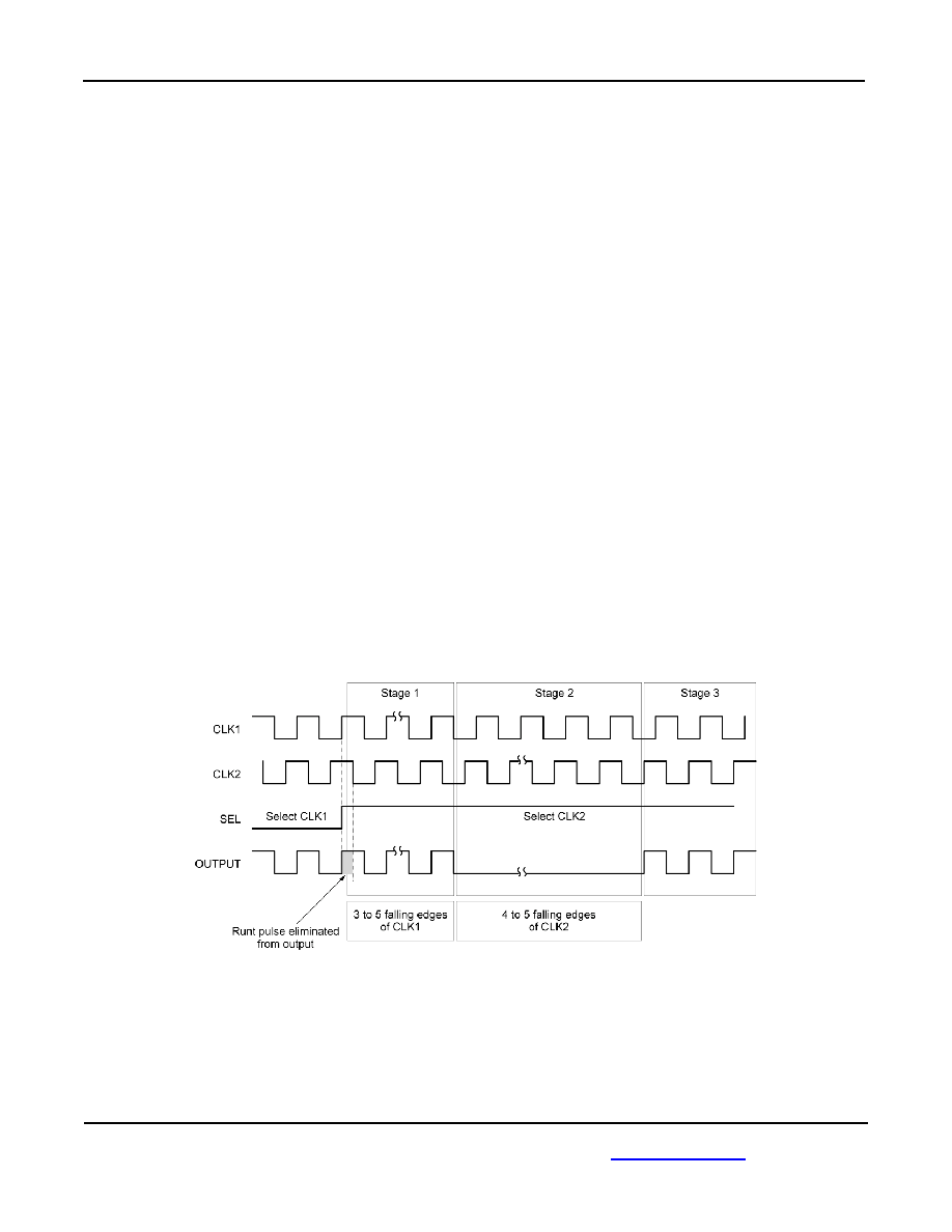
RPE and FSI Functionality
The basic operation of the RPE MUX and FSI
functionality is described with the following four case
descriptions. All descriptions are related to the true
inputs and outputs. The primary (or selected) clock
is called CLK1; the secondary (or alternate) clock is
called CLK2. Due to the totally asynchronous
relation of the IN and SEL signals and an additional
internal protection against metastability, the number
of pulses required for the operations described in
cases 1-4 can vary within certain limits. Refer to
“Timing Diagrams” for more detailed information.
Case #1 Two Normal Clocks and RPE Enabled
In this case, the frequency difference between the
two running clocks IN0 and IN1 must not be greater
than 1.5:1. For example, if the IN0 clock is 500MHz,
the IN1 clock must be within the range of 334MHz to
750MHz.
If the SEL input changes state to select the alternate
clock, then the switchover from CLK1 to CLK2 will
occur in three stages.
Stage 1: The output will continue to follow
CLK1 for a limited number of pulses.
Stage 2: The output will remain LOW for a
limited number of pulses of CLK2.
Stage 3: The output follows CLK2.
Timing Diagram 1
相关PDF资料 |
PDF描述 |
|---|---|
| SY89844UMG TR | IC MUX LVDS RPE 2:1 PREC 24-MLF |
| SY89845UMG TR | IC MUX CML RPE 2:1 PREC 24-MLF |
| SY89846UMG TR | IC CLK BUFF MUX 2:5 2GHZ 32-MLF |
| SY89847UMG TR | IC CLK BUFF MUX 2:5 2GHZ 32-MLF |
| SY89850UMG TR | IC DRVR/RCVR LVPECL PREC 8-MLF |
相关代理商/技术参数 |
参数描述 |
|---|---|
| SY89844U | 制造商:MICREL 制造商全称:Micrel Semiconductor 功能描述:Precision LVDS Runt Pulse Eliminator 2:1 MUX with 1:2 Fanout and Internal Termination |
| SY89844U_10 | 制造商:MICREL 制造商全称:Micrel Semiconductor 功能描述:Precision LVDS Runt Pulse Eliminator 2:1 |
| SY89844UMG | 功能描述:编码器、解码器、复用器和解复用器 2.5V 2:1 RPE/FSI LVDS MUX w/ 1:2 Fanout (I Temp, Green) RoHS:否 制造商:Micrel 产品:Multiplexers 逻辑系列:CMOS 位数: 线路数量(输入/输出):2 / 12 传播延迟时间:350 ps, 400 ps 电源电压-最大:2.625 V, 3.6 V 电源电压-最小:2.375 V, 3 V 最大工作温度:+ 85 C 安装风格:SMD/SMT 封装 / 箱体:QFN-44 封装:Tray |
| SY89844UMG TR | 功能描述:编码器、解码器、复用器和解复用器 2.5V 2:1 RPE/FSI LVDS MUX w/ 1:2 Fanout (I Temp, Green) RoHS:否 制造商:Micrel 产品:Multiplexers 逻辑系列:CMOS 位数: 线路数量(输入/输出):2 / 12 传播延迟时间:350 ps, 400 ps 电源电压-最大:2.625 V, 3.6 V 电源电压-最小:2.375 V, 3 V 最大工作温度:+ 85 C 安装风格:SMD/SMT 封装 / 箱体:QFN-44 封装:Tray |
| SY89844UMGTR | 制造商:MICREL 制造商全称:Micrel Semiconductor 功能描述:Precision LVDS Runt Pulse Eliminator 2:1 MUX with 1:2 Fanout and Internal Termination |
发布紧急采购,3分钟左右您将得到回复。