- 您现在的位置:买卖IC网 > PDF目录69401 > TA7291ASJ BRUSH DC MOTOR CONTROLLER, 1.2 A, PSIP9 PDF资料下载
参数资料
| 型号: | TA7291ASJ |
| 元件分类: | 运动控制电子 |
| 英文描述: | BRUSH DC MOTOR CONTROLLER, 1.2 A, PSIP9 |
| 封装: | SIP-9 |
| 文件页数: | 14/14页 |
| 文件大小: | 310K |
| 代理商: | TA7291ASJ |
TA7291AP/AS(J)/AF
2003-02-14
9
Notes
Power On/Off
At power on, VCC must be applied simultaneously or before VS. At power off, VCC must be removed
simultaneously or after VS.
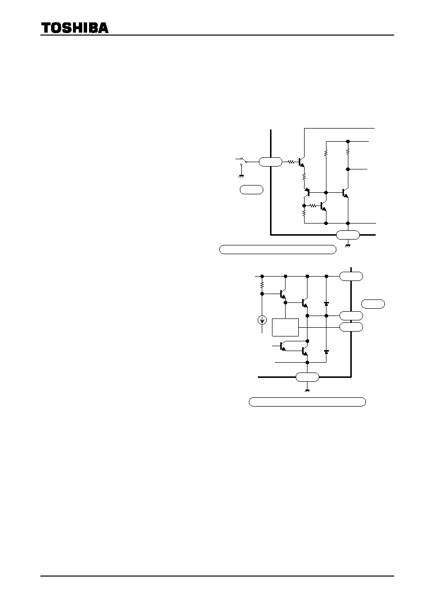
Input Circuit
A logic high on the VIN pin activates the input
circuit as shown in the figure.
When a voltage greater than or equal to VIN (high)
is applied to the pin, the circuit is active. When a
voltage less than or equal to VIN (low) is applied to
the pin or the pin is grounded, the circuit is
inactive.
When the pin is high, the input current IIN flows
into the input circuit. So, be careful about the
output impedance of the first stage.
The input hysteresis is 0.7 V (typ.). At power on
(VCC), set both input pins IN1 and IN2 to low.
Output Circuit
Output high voltage
Operation based on the Vref voltage
The Vref voltage is increased by twice the value
of VBE (small signal) in the Vref circuit. Then,
the voltage is applied to the base A of Q2 (power
transistor 2). As a result, the voltage which is
reduced by the value of VBE (Q2) appears on the
VOUT pin.
VOUT = Vref + 2VBE-VBE (Q2) ~- Vref + 0.7 V
Vref pin
The Vref pin must not be left open when unused.
In this case, connect it via a protection resistor
(3 kW or more) to the VS pin. Otherwise, it
might cause oscillation.
Vref must be VS.
Protection Features
Overcurrent Protection Circuit
The overcurrent protection circuit detects a current flowing through the upper power transistor. If the
current exceeds a predetermined value (about 2.5 A), the circuit turns all the power transistors off.
However, it does not always prevent overcurrent. If an output pin is shorted or grounded, the IC might be
destroyed before operation of the overcurrent protection circuit. So, be sure to connect a resistor or fuse to
the power supply (VS) line. (See “Application Circuit.”)
Thermal Shutdown Circuit
If the chip temperature exceeds a predetermined limit (about 170°C), the thermal shutdown circuit turns
all the power transistors off.
or
VIN
6/1/9
4.
5k
W
5/9/7
1 k
W
10
k
W
10
k
W
1.
3k
W
1/5/1
VIN
5 k
W
VCC standby
TA7291AP/TA7291AS (J)/TA7291AF
or
A
1/5/1
VOUT
Q1
10/3/13
2/7/4
4/8/5
8/6/15
Vref
circuit
Q2
TA7291AP/TA7291AS (J)/TA7291AF
相关PDF资料 |
PDF描述 |
|---|---|
| TA7291AS | BRUSH DC MOTOR CONTROLLER, 1.2 A, PSIP9 |
| TA7291AF | BRUSH DC MOTOR CONTROLLER, 1.2 A, PDSO16 |
| TA7291AP | BRUSH DC MOTOR CONTROLLER, 2 A, PSFM10 |
| TA7291F | BRUSH DC MOTOR CONTROLLER, 1.2 A, PDSO18 |
| TA7291SG | BRUSH DC MOTOR CONTROLLER, 1.2 A, PSIP9 |
相关代理商/技术参数 |
参数描述 |
|---|---|
| TA7291F | 制造商:TOSHIBA 制造商全称:Toshiba Semiconductor 功能描述:BRIDGE DRIVER |
| TA7291F/FG | 制造商:TOSHIBA 制造商全称:Toshiba Semiconductor 功能描述:BRIDGE DRIVER |
| TA7291FG | 制造商:TOSHIBA 制造商全称:Toshiba Semiconductor 功能描述:BRIDGE DRIVER |
| TA7291FG(5) | 制造商:Toshiba America Electronic Components 功能描述: |
| TA7291FG(5,EL) | 功能描述:马达/运动/点火控制器和驱动器 BRIDGE DRIVER BRUSHED DC MOTOR RoHS:否 制造商:STMicroelectronics 产品:Stepper Motor Controllers / Drivers 类型:2 Phase Stepper Motor Driver 工作电源电压:8 V to 45 V 电源电流:0.5 mA 工作温度:- 25 C to + 125 C 安装风格:SMD/SMT 封装 / 箱体:HTSSOP-28 封装:Tube |
发布紧急采购,3分钟左右您将得到回复。