- 您现在的位置:买卖IC网 > PDF目录98156 > TA8225H 45 W, 1 CHANNEL, AUDIO AMPLIFIER, PZFM17 PDF资料下载
参数资料
| 型号: | TA8225H |
| 元件分类: | 音频/视频放大 |
| 英文描述: | 45 W, 1 CHANNEL, AUDIO AMPLIFIER, PZFM17 |
| 封装: | HZIP-17 |
| 文件页数: | 11/15页 |
| 文件大小: | 1315K |
| 代理商: | TA8225H |
TA8225H/L
2002-10-30
5
(2) Input offset voltage
Input offset voltage is increased by as many times as a gain and appears as output offset voltage.
Input offset voltage is affected by an external resistor in addition to properness of pair of capacitor in IC.
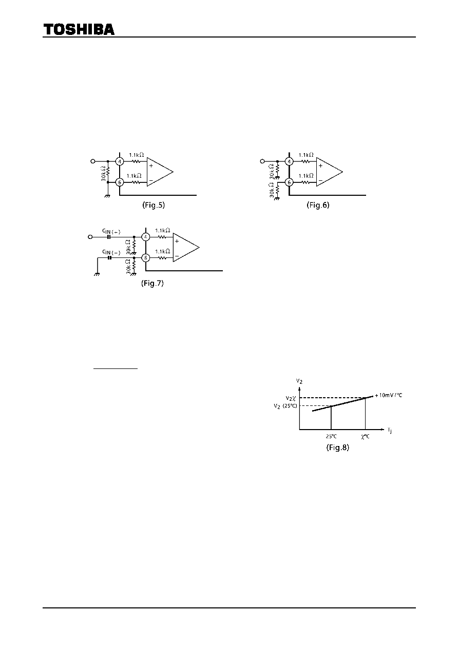
An example of a general application circuit is shown in (Fig.5). In this case, input to the differential amplifier
composing the buffer amplifier is decided to be 30k + 1.1k = 31.1k at the in (+) side and 1.1k at the in (-)
side. Therefore a rising difference of about 30 times between the in (+) side and the in (-) side.
So, to fit input offset voltages, it is possible to suppress the input offset voltage by adjusting it to 31.1k both
at the in (+) and in (-) sides according to the application example shown in (Fig.6). As input coupling
capacitors are used in actual set, the circuit shown in (Fig.7) is considered. In this case, it is necessary to
take the utmost care of proper pair of CIN (+) and CIN (-).
Pop noise level affected by input offset voltage shall be checked on an actually mounted set.
4. Junction temperature detecting pin(2)
Using temperature characteristic of a band gap circuit and in proportion to junction temperature, pin(2) DC
voltage: V2 rises at about ±10mV / °C temperature characteristic. So, the relation between V2 at Tj = 25°C and
V2χ at Tj =χ°C is decided by the following expression:
C)
25(
C
10mV /
C)
(25
2
V
2
V
C)
(
j
T
°
+
°
-
c
=
°
c
In deciding a heat sink suze, a junction temperature can be
easily made clear by measuring voltage at this pin while a
backside temperature of IC was so far measured using a
thermocouple type thermometer.
相关PDF资料 |
PDF描述 |
|---|---|
| TA8227P | 3 W, 2 CHANNEL, AUDIO AMPLIFIER, PDIP12 |
| TA8229K | 2.5 W, 2 CHANNEL, AUDIO AMPLIFIER, PSFM15 |
| TA8229K | 4.6 W, 2 CHANNEL, AUDIO AMPLIFIER, PSIP15 |
| TA8231LQ | 42 W, 2 CHANNEL, AUDIO AMPLIFIER, PSFM17 |
| TA8231LQ | 42 W, 2 CHANNEL, AUDIO AMPLIFIER, PSFM17 |
相关代理商/技术参数 |
参数描述 |
|---|---|
| TA8225HQ | 制造商:TOSHIBA 制造商全称:Toshiba Semiconductor 功能描述:45W BTL Audio Amplifier |
| TA8225L | 制造商:TOSHIBA 制造商全称:Toshiba Semiconductor 功能描述:45W BTL AUDIO AMPLIFIER |
| TA8225LQ | 制造商:Toshiba America Electronic Components 功能描述: |
| TA8227 | 制造商:TOSHIBA 制造商全称:Toshiba Semiconductor 功能描述:LOW FREQUENCY POWER AMPLIFIER |
| TA8227AP | 制造商:UTC-IC 制造商全称:UTC-IC 功能描述:LOW FREQUENCY POWER AMPLIFIER |
发布紧急采购,3分钟左右您将得到回复。