- 您现在的位置:买卖IC网 > PDF目录98156 > TA8227P 3 W, 2 CHANNEL, AUDIO AMPLIFIER, PDIP12 PDF资料下载
参数资料
| 型号: | TA8227P |
| 元件分类: | 音频/视频放大 |
| 英文描述: | 3 W, 2 CHANNEL, AUDIO AMPLIFIER, PDIP12 |
| 封装: | 0.300 INCH, 2.54 MM PITCH, HEAT SINK, PLASTIC, DIP-12 |
| 文件页数: | 5/11页 |
| 文件大小: | 472K |
| 代理商: | TA8227P |
TA8227P
2002-03-05
3
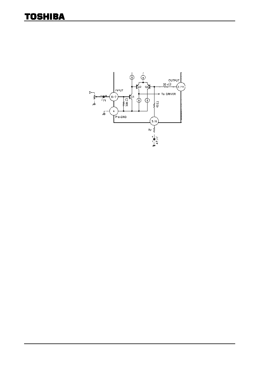
3. Input stage
The input circuit of this IC is as shown in Figure 2.
PNP Tr: Q1 is provided in the input circuit so as to make its usage possible without the input coupling
capacitor.
However, at pin 6 and 7, max 60 mV offset voltage is produced.
Application after checking volume slide noise is recommended.
For cutting the volume slide noise, insert the input capacitor: CIN in series to interrupt the DC component.
Figure 2
4. Oscillation preventive measures (Note 1)
For oscillation preventive capacitor C6 and C7 between the output terminal and GND, it is recommended to
use polyester film capacitor having good characteristics for temperature and for high frequency.
Since the characteristics of the capacitor is liable to be influenced by the temperature, use this capacitor
after the temperature test to check the oscillation allowance.
In addition, as the position of the electrolytic capacitor has a remarkable influence on the oscillation,
connect C10 to VCC at the nearest possible position from power GND.
At using this application with the voltage gain reduced, oscillation is liable to be produced. Apply the
capacitor after checking enough for its capacity, type and mounting position.
Note 1: As the oscillation allowance varies according to the printed pattern layout, the standard printed board
of TOSHIBA is recommended to be referred to design it.
5. Power ON/OFF switch
There is power ON/OFF switch at pin 1. However, output power is changed by pin 1 supply voltage when
pin 1 supply voltage is not same pin 12 supply voltage, after referring to attached data, select pin 1 supply
voltage.
6. Input voltage
When the excessive signal is input, turning-up is produced in the clip waveform. The turning-up point is
Vin = 300 mVrms (typ.) : VCC = 9 V, RL = 4 , f = 1 kHz: Enough care must be taken for this phenomenon.
相关PDF资料 |
PDF描述 |
|---|---|
| TA8229K | 2.5 W, 2 CHANNEL, AUDIO AMPLIFIER, PSFM15 |
| TA8229K | 4.6 W, 2 CHANNEL, AUDIO AMPLIFIER, PSIP15 |
| TA8231LQ | 42 W, 2 CHANNEL, AUDIO AMPLIFIER, PSFM17 |
| TA8231LQ | 42 W, 2 CHANNEL, AUDIO AMPLIFIER, PSFM17 |
| TA8233AH | 30 W, 2 CHANNEL, AUDIO AMPLIFIER, PSFM17 |
相关代理商/技术参数 |
参数描述 |
|---|---|
| TA8229 | 制造商:UTC-IC 制造商全称:UTC-IC 功能描述:LOW FREQUENCY POWER AMPLIFIER |
| TA8229K | 制造商:TOSHIBA 制造商全称:Toshiba Semiconductor 功能描述:LOW FREQUENCY POWER AMPLIFIER |
| TA8231 | 制造商:TOSHIBA 制造商全称:Toshiba Semiconductor 功能描述:42W BTL x 2CH AUDIO POWER IC |
| TA8231L | 制造商:TOSHIBA 制造商全称:Toshiba Semiconductor 功能描述:42W BTL x 2CH AUDIO POWER IC |
| TA8231LQ | 制造商:TOSHIBA 制造商全称:Toshiba Semiconductor 功能描述:42W BTL 】 2CH Audio Power IC |
发布紧急采购,3分钟左右您将得到回复。