- 您现在的位置:买卖IC网 > PDF目录98159 > TAS5015IPFB (TEXAS INSTRUMENTS INC) SPECIALTY CONSUMER CIRCUIT, PQFP48 PDF资料下载
参数资料
| 型号: | TAS5015IPFB |
| 厂商: | TEXAS INSTRUMENTS INC |
| 元件分类: | 消费家电 |
| 英文描述: | SPECIALTY CONSUMER CIRCUIT, PQFP48 |
| 封装: | PLASTIC, TQFP-48 |
| 文件页数: | 17/20页 |
| 文件大小: | 266K |
| 代理商: | TAS5015IPFB |
TAS5015
SLES017 SEPTEMBER 2001
6
www.ti.com
functional description (continued)
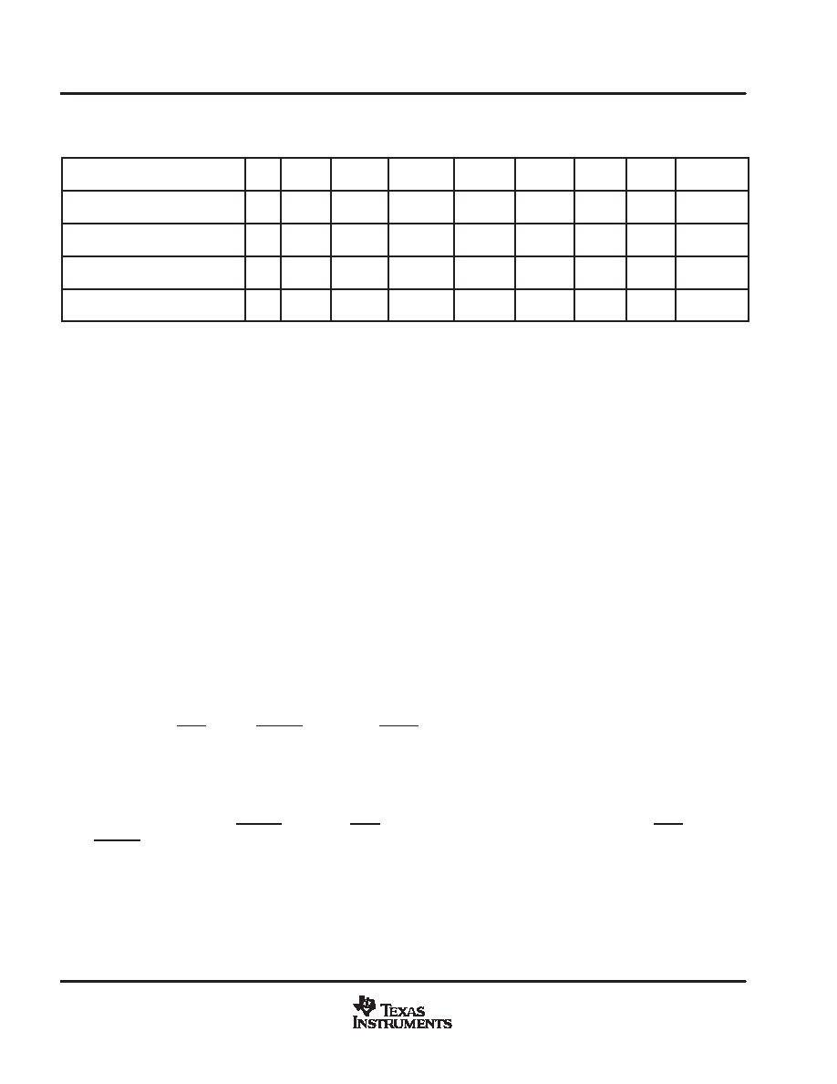
Table 1. External Clock and External PLL Functions (Continued)
DESCRIPTION
M_S
DBSPD
DEM_EN
DEM_SEL
MCLK_IN
(MHz)
HFCLK
(MHz)
SCLK
(MHz)
LRCLK
(kHz)
MCLK_OUT
(MHz)
External PLL, slave, double speed
(see Notes 3, 4, and 5)
0
1
0
22.5792
90.3168
5.6448
88.2
22.5792
External PLL, slave, double speed
(see Notes 3, 4, and 5)
0
1
0
24.576
98.304
6.144
96
24.576
External PLL, slave, quad speed
(see Notes 3, 4, and 5)
0
22.5792
90.3168
11.2896
176.4
22.5792
External PLL, slave, quad speed
(see Notes 3, 4, and 5)
0
24.576
98.304
12.288
192
24.576
NOTES:
3. External MCLK connected to MCLK_IN input
4. SCLK and LRCLK are inputs
5. MCLK_OUT is a buffered version of the external MCLK input
external PLL
For the highest system performance, an external PLL must be used with the TAS5015. For normal-speed mode,
the external PLL input (HFCLK) must be 2048 Fs, for double-speed mode HFCLK must be 1024 Fs, and for
quad-speed mode HFCLK must be 512 Fs.
digital interpolation filter
The 24-bit high-performance linear phase FIR interpolation filter up-samples the input digital data at a rate of
two times (quad-speed mode = 176.4 kHz or 192 kHz), four times (double-speed mode = 88.2 kHz or 96 kHz),
or eight times (normal mode = 44.1 kHz or 48 kHz) the incoming sample rate. This filter provides low pass-band
ripple and optimized time domain transient response for accurate music reproduction.
digital PWM modulator
The interpolation filter output is sent to the digital PWM modulator. This modulator consists of a high-
performance fourth order digital-noise shaper and a PCM-to-PWM converter. Following the noise shaper, the
PCM signal is fed into a low distortion PCM-to-PWM conversion block, buffered, and output from the chip. The
modulation scheme is based on a 2-state control of the H-bridge output.
control, status, and operational modes
The TAS5015 control section consists of several control-input pins. Three serial mode pins (MOD0, MOD1, and
MOD2) are provided to select various serial data formats. During normal operating conditions if any of the
MOD0, MOD1, or MOD2 pins changes state, a reset sequence is initiated. Also provided are separate
power-down (PDN), reset (RESET), and mute (MUTE) pins.
power up
At power up, the VALID_L and VALID_R pins are asserted low and the PWM outputs go to the hard mute state
in which the P outputs are held low and the M outputs are held high. Following initialization, the TAS5015 comes
up in the operational state (differential PWM audio). There are two cases of power-up timing. The first case is
shown in Figure 1 with RESET preceding PDN. The second case is shown in Figure 2 with PDN preceding
RESET.
相关PDF资料 |
PDF描述 |
|---|---|
| TAS5015PFBG4 | SPECIALTY CONSUMER CIRCUIT, PQFP48 |
| TAS5026APAGG4 | SPECIALTY CONSUMER CIRCUIT, PQFP64 |
| TAS5026APAG | SPECIALTY CONSUMER CIRCUIT, PQFP64 |
| TAS5026APAGR | SPECIALTY CONSUMER CIRCUIT, PQFP64 |
| TAS5026APAGRG4 | SPECIALTY CONSUMER CIRCUIT, PQFP64 |
相关代理商/技术参数 |
参数描述 |
|---|---|
| TAS5015PFB | 功能描述:音频 DSP Digital Audio PWM Processor RoHS:否 制造商:Texas Instruments 工作电源电压: 电源电流: 工作温度范围: 安装风格: 封装 / 箱体: 封装:Tube |
| TAS5015PFBG4 | 功能描述:音频 DSP Digital Audio PWM Processor RoHS:否 制造商:Texas Instruments 工作电源电压: 电源电流: 工作温度范围: 安装风格: 封装 / 箱体: 封装:Tube |
| TAS5026 | 制造商:TI 制造商全称:Texas Instruments 功能描述:SIX CHANNEL DIGITAL AUDIO PWM PROCESSOR |
| TAS5026A | 制造商:TI 制造商全称:Texas Instruments 功能描述:Six-Channel Digital Audio PWM Processor |
| TAS5026APAG | 功能描述:音频 DSP 6Ch Dig Aud PWM Proc RoHS:否 制造商:Texas Instruments 工作电源电压: 电源电流: 工作温度范围: 安装风格: 封装 / 箱体: 封装:Tube |
发布紧急采购,3分钟左右您将得到回复。