- 您现在的位置:买卖IC网 > PDF目录98159 > TAS5026PAGR (TEXAS INSTRUMENTS INC) SPECIALTY CONSUMER CIRCUIT, PQFP64 PDF资料下载
参数资料
| 型号: | TAS5026PAGR |
| 厂商: | TEXAS INSTRUMENTS INC |
| 元件分类: | 消费家电 |
| 英文描述: | SPECIALTY CONSUMER CIRCUIT, PQFP64 |
| 封装: | GREEN, PLASTIC, TQFP-64 |
| 文件页数: | 5/52页 |
| 文件大小: | 886K |
| 代理商: | TAS5026PAGR |
第1页第2页第3页第4页当前第5页第6页第7页第8页第9页第10页第11页第12页第13页第14页第15页第16页第17页第18页第19页第20页第21页第22页第23页第24页第25页第26页第27页第28页第29页第30页第31页第32页第33页第34页第35页第36页第37页第38页第39页第40页第41页第42页第43页第44页第45页第46页第47页第48页第49页第50页第51页第52页
Architecture Overview
8
SLES041B—November 2002
TAS5026
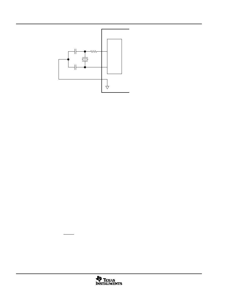
XO
TAS5026
OSC
MACRO
rd
C1
XI
C2
AVSS
rd = Drive level control resistor – crystal vendor specified
CL = Crystal load capacitance (capacitance of circuitry between the two terminals of the crystal)
CL = (C1 x C2 )/(C1 + C2 ) + CS (where CS = board stray capacitance ~ 3 pF)
Example: Vendor recommended CL = 18 pF, CS = 3 pF ≥ C1 = C2 = 2 x (18–3) = 30 pF
Figure 2–1. Crystal Circuit
2.1.4 Clock Slave Mode
In the slave mode (M_S = 0), the master clock, LRCLK, and SCLK are inputs to the TAS5026. The master clock
is supplied through the MCLK_IN terminal.
As in the master mode, the TAS5026 device developed its internal timing from internal phase-locked loop
(PLL). The reference clock for the PLL is provided by the input to the MCLK_IN terminal. This input is at a
frequency of 256 times (128 in quad mode) the input data rate. The SCLK frequency is 48 or 64 times the data
sample rate. The LRCLK frequency is the data sample rate. The TAS5026 does not require any specific phase
relationship between SRCLK and MCLK_IN, but there must be synchronization.
The TAS5026 monitors the relationship between MCLK, SCLK and LRCLK. The TAS5026 detects if any of
the three clocks are absent, if LRCLK rate changes more the
±10 MCLK cycles since the last device reset or
clock error recovery, or if MCLK frequency is changing substantially with respect to the PLL frequency. When
a clock error is detected the TAS5026 performs a clock error recovery sequence. If one or more of the clock
signals are absent, the TAS5026 is held with the outputs in hard mute until the clock is resumed. Once the
clock is resumed, the clock error recover sequence is completed.
NOTE:
The detection of a clock error causes the TAS5026 to perform an immediate hard mute and
suspension of all processes. This abrupt transition can produce a faint click as the outputs are
muted.
Since the clocks are removed when changing media or during input selection, it is possible to use this
knowledge to completely eliminate clicks in these conditions. In this case, the click is prevented by muting the
outputs by using the MUTE terminal or the I2C /MUTE command 43 ms in advance of the clocks being
removed.
In the slave mode, MCLK_OUT is driven low.
Table 2–2 shows all the possible master and slave modes. When operating in quad mode (Fs = 176.4 kHz
or 192 kHz), the device works in slave mode only with MCLK_IN = 128 Fs.
Table 2–3 shows the clocks speed for normal, double and quad modes.
相关PDF资料 |
PDF描述 |
|---|---|
| TAS5026PAG | SPECIALTY CONSUMER CIRCUIT, PQFP64 |
| TAS5026PAGG4 | SPECIALTY CONSUMER CIRCUIT, PQFP64 |
| TAS5026IPAGRG4 | SPECIALTY CONSUMER CIRCUIT, PQFP64 |
| TAS5026IPAGR | SPECIALTY CONSUMER CIRCUIT, PQFP64 |
| TAS5026IPAG | SPECIALTY CONSUMER CIRCUIT, PQFP64 |
相关代理商/技术参数 |
参数描述 |
|---|---|
| TAS5026PAGRG4 | 功能描述:多媒体杂项 Dig Aud PWM Proc RoHS:否 制造商:Texas Instruments 类型: 通道数量: 转换速率:540 Mbps 分辨率: 封装 / 箱体:SOIC-16 封装:Tube |
| TAS5028 | 制造商:TI 制造商全称:Texas Instruments 功能描述:8 Channel Digital Audio PWM Processor |
| TAS5028-5122C6EVM | 功能描述:音频 IC 开发工具 TAS5028-5122C6 Eval Mod RoHS:否 制造商:Texas Instruments 产品:Evaluation Kits 类型:Audio Amplifiers 工具用于评估:TAS5614L 工作电源电压:12 V to 38 V |
| TAS5028A | 制造商:TI 制造商全称:Texas Instruments 功能描述:8 Channel Digital Audio PWM Processor |
| TAS5028APAG | 功能描述:音频放大器 8Ch Dig Aud PWM Proc RoHS:否 制造商:STMicroelectronics 产品:General Purpose Audio Amplifiers 输出类型:Digital 输出功率: THD + 噪声: 工作电源电压:3.3 V 电源电流: 最大功率耗散: 最大工作温度: 安装风格:SMD/SMT 封装 / 箱体:TQFP-64 封装:Reel |
发布紧急采购,3分钟左右您将得到回复。