- 您现在的位置:买卖IC网 > PDF目录98161 > TAS5110DAPR (TEXAS INSTRUMENTS INC) 50 W, 2 CHANNEL, AUDIO AMPLIFIER, PDSO32 PDF资料下载
参数资料
| 型号: | TAS5110DAPR |
| 厂商: | TEXAS INSTRUMENTS INC |
| 元件分类: | 音频/视频放大 |
| 英文描述: | 50 W, 2 CHANNEL, AUDIO AMPLIFIER, PDSO32 |
| 封装: | GREEN, PLASTIC, HTSSOP-32 |
| 文件页数: | 17/20页 |
| 文件大小: | 336K |
| 代理商: | TAS5110DAPR |
TAS5110
SLES028A MAY 2002 REVISED SEPTEMBER 2002
6
www.ti.com
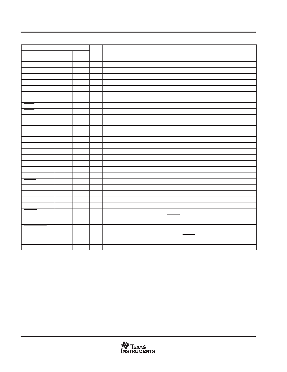
Terminal Functions
TERMINAL
NAME
DAP
NO.
DAD
NO.
I/O
DESCRIPTION
BIAS_A
11
6
I
Connect external resistor to DVSS.
BIAS_B
12
5
I
Connect external resistor to DVSS.
BOOTSTRAPA
30
19
O
Bootstrap capacitor pin for H-bridge A
BOOTSTRAPB
19
30
O
Bootstrap capacitor pin for H-bridge B
DVDD
6
11
I
3.3-V digital voltage supply for logic
DVSS
7, 8, 9
8, 9,
10
I
Digital ground for logic is internally connected to PVSS. All three pins must be tied
together but not connected externally to PVSS. See Figure 5.
ERR1
3
14
O
Error/warning report indicator. This output is open drain with internal pullup resistor.
ERR0
4
13
O
Error/warning report indicator. This output is open drain with internal pullup resistor.
LDROUTA
31
18
O
Low voltage drop-out regulator output A (not to be used to supply current to external
circuitry)
LDROUTB
18
31
O
Low voltage drop-out regulator output B (not to be used to supply current to external
circuitry)
OUTPUTA
26, 27
22, 23
O
H-bridge output A
OUTPUTB
22, 23
26, 27
O
H-bridge output B
PVDDA1
28, 29
20, 21
I
High voltage power supply, H-bridge A
PVDDA2
32
17
I
High voltage power supply for low-dropout voltage regulator A-side
PVDDB1
20, 21
28, 29
I
High voltage power supply, H-bridge B
PVDDB2
17
32
I
High voltage power supply for low-dropout voltage regulator B-side
PVSS
24, 25
I
High voltage power supply ground
PWDN
13
4
I
Power down = 0, normal mode = 1
PWM_AM
2
15
I
PWM input A()
PWM_AP
1
16
I
PWM input A(+)
PWM_BP
16
1
I
PWM input B(+)
PWM_BM
15
2
I
PWM input B()
RESET
14
3
I
Reset and mute mode = 0, normal mode = 1, when in reset mode, H-bridge MOSFETs are
in low-low output state. Asserting the RESET signal low causes all fault conditions to be
cleared.
SHUTDOWN
5
12
O
Device is in shutdown due to fault condition, normal mode = 1, shutdown = 0, when
device is in shutdown mode the H-bridge MOSFETs are in low-low output state. The
latched output can be cleared by asserting the RESET signal. This output is open drain
with internal pullup resistor.
VRFILT
10
7
O
A filter capacitor must be added between VRFILT and DVSS pins.
NOTE: The four PWM inputs: PWM_AP, PWM_AM, PWM_BP, and PWM_BM must always be connected to the TAS50xx output pins, and never
left floating. Floating PWM input pins causes an illegal PWM input state signal to be asserted.
Dual pins: OUTPUTA, OUTPUTB, PVDDA1, and PVDDB1 must have both pins connected externally to the same point on the circuit board,
respectively. Both PVSS pins must also be connected together externally. These multiple pins are for the high-current DMOS output
devices. Failure to connect all the multiple pins to the same respective node results in excessive current flow in the internal bond wires
and can cause the device to fail. All electrical characteristics are specified and measured with all of the multiple pins connected to the same
node, respectively.
相关PDF资料 |
PDF描述 |
|---|---|
| TAS5110IDAPR | 50 W, 2 CHANNEL, AUDIO AMPLIFIER, PDSO32 |
| TAS5110DADRG4 | 50 W, 2 CHANNEL, AUDIO AMPLIFIER, PDSO32 |
| TAS5110IDAD | 50 W, 2 CHANNEL, AUDIO AMPLIFIER, PDSO32 |
| TAS5110IDADR | 50 W, 2 CHANNEL, AUDIO AMPLIFIER, PDSO32 |
| TAS5111ADADRG4 | 93 W, 1 CHANNEL, AUDIO AMPLIFIER, PDSO32 |
相关代理商/技术参数 |
参数描述 |
|---|---|
| TAS5110DAPRG4 | 功能描述:音频放大器 Dig Amp Power Stage RoHS:否 制造商:STMicroelectronics 产品:General Purpose Audio Amplifiers 输出类型:Digital 输出功率: THD + 噪声: 工作电源电压:3.3 V 电源电流: 最大功率耗散: 最大工作温度: 安装风格:SMD/SMT 封装 / 箱体:TQFP-64 封装:Reel |
| TAS5110IDAD | 制造商:TI 制造商全称:Texas Instruments 功能描述:TRUE DIGITAL AUDIO AMPLIFIER TAS5110 PWM POWER OUTPUT STAGE |
| TAS5110IDADR | 制造商:TI 制造商全称:Texas Instruments 功能描述:TRUE DIGITAL AUDIO AMPLIFIER TAS5110 PWM POWER OUTPUT STAGE |
| TAS5110IDAP | 制造商:TI 制造商全称:Texas Instruments 功能描述:TRUE DIGITAL AUDIO AMPLIFIER TAS5110 PWM POWER OUTPUT STAGE |
| TAS5110IDAPR | 制造商:TI 制造商全称:Texas Instruments 功能描述:TRUE DIGITAL AUDIO AMPLIFIER TAS5110 PWM POWER OUTPUT STAGE |
发布紧急采购,3分钟左右您将得到回复。