- 您现在的位置:买卖IC网 > PDF目录98161 > TAS5111DADRG4 (TEXAS INSTRUMENTS INC) 93 W, 2 CHANNEL, AUDIO AMPLIFIER, PDSO32 PDF资料下载
参数资料
| 型号: | TAS5111DADRG4 |
| 厂商: | TEXAS INSTRUMENTS INC |
| 元件分类: | 音频/视频放大 |
| 英文描述: | 93 W, 2 CHANNEL, AUDIO AMPLIFIER, PDSO32 |
| 封装: | GREEN, PLASTIC, HTSSOP-32 |
| 文件页数: | 2/18页 |
| 文件大小: | 325K |
| 代理商: | TAS5111DADRG4 |
TAS5111
SLES049D JULY 2003 REVISED MARCH 2004
www.ti.com
10
THEORY OF OPERATION
POWER SUPPLIES
The power device only requires two supply voltages,
GVDD and PVDD_X.
GVDD is the gate drive supply for the device, regulated
internally down to approximately 12 V, and decoupled with
regards to board GND on the GREG pins through an
external capacitor. GREG powers both the low side and
high side via a bootstrap step-up conversion. The
bootstrap supply is charged after the first low-side turnon
pulse. Internal digital core voltage DREG is also derived
from GVDD and regulated down by internal LDRs to 3.3 V.
The gate-driver LDR can be bypassed for reducing idle
loss in the device by shorting GREG to GVDD and directly
feeding in 12 V. This can be useful in an application where
thermal conduction of heat from the device is difficult.
Bypassing the LDR reduces dissipation by approximately
1 W at 30-V GVDD input.
PVDD_X is the H-bridge power supply pin. Two power
pins exist for each half-bridge to handle the current density.
It is important that the circuitry recommendations around
the PVDD_X pins are followed carefully both topology-
and layout-wise. For topology recommendations, see the
Typical
System
Configuration
section.
For
layout
recommendations, see the reference design layout for the
TAS5111. Following these recommendations is important
for parameters like EMI, reliability, and performance.
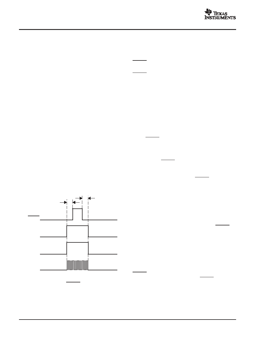
POWERING UP
RESET
GVDD
PVDD_x
PWM_xP
> 1 ms
NOTE: PVDD should not be powered up before GVDD.
During power up when RESET is asserted LOW, all
MOSFETs are turned off and the two internal half-bridges
are in the high-impedance state (Hi-Z). The bootstrap
capacitors supplying high-side gate drive are at this point
not charged. To comply with the click and pop scheme and
use of non-TI TDAA modulators, it is recommended to use
a 4-k
pulldown resistor on each PWM output node to
ground. This precharges the bootstrap supply capacitors
and discharges the output filter capacitor (see the Typical
TAS5111 Application Configuration section).
After GVDD has been applied, it takes approximately 800
s to fully charge the BST capacitor. Within this time,
RESET must be kept low. After approximately 1 ms, the
back-end bootstrap capacitor is charged.
RESET can now be released if the modulator is powered
up and streaming valid PWM signals to the back-end
PWM_xP. Valid means a switching PWM signal which
complies with the frequency and duty cycle ranges stated
in the Recommended Operating Conditions.
A constant HIGH dc level on the PWM_xP is not permitted,
because it would force the high-side MOSFET ON until it
eventually runs out of BST capacitor energy and might
damage the device.
An unknown state of the PWM output signals from the
modulator is not permitted, which in practice means that
the PWM processor must be powered up and initialized
before RESET is de-asserted HIGH to the back end.
POWERING DOWN
For power down of the back end, an opposite approach is
necessary. The RESET must be asserted LOW before the
valid PWM signal is removed.
When TI TDAA modulators are used with TI TDAA back
ends, the correct timing control of RESET and PWM_xP
is performed by the modulator.
PRECAUTION
The TAS5111 must always start up in the high-impedance
(Hi-Z) state. In this state, the bootstrap (BST) capacitor is
precharged by a resistor on each PWM output node to
ground. See the system configuration. This ensures that
the back end is ready for receiving PWM pulses, indicating
either HIGH- or LOW-side turnon after RESET is
de-asserted to the back end.
With the following pulldown resistor and BST capacitor
size, the charge time is:
C = 33 nF, R = 4.7 k
R
× C × 5 = 775.5 s
After GVDD has been applied, it takes approximately 800
s to fully charge the BST capacitor. During this time,
RESET must be kept low. After approximately 1 ms, the
back-end BST is charged and ready. RESET can now be
released if the PWM modulator is ready and is streaming
valid PWM signals to the back end. Valid PWM signals are
switching PWM signals with a frequency between
350400 kHz. A constant HIGH level on the PWM+ would
force the high side MOSFET ON until it eventually ran out
of BST capacitor energy. Putting the device in this
condition should be avoided.
相关PDF资料 |
PDF描述 |
|---|---|
| TAS5111DADG4 | 93 W, 2 CHANNEL, AUDIO AMPLIFIER, PDSO32 |
| TAS5112ADFD | 62 W, 2 CHANNEL, AUDIO AMPLIFIER, PDSO56 |
| TAS5112ADCAG4 | 62 W, 2 CHANNEL, AUDIO AMPLIFIER, PDSO56 |
| TAS5112ADCARG4 | 62 W, 2 CHANNEL, AUDIO AMPLIFIER, PDSO56 |
| TAS5112ADCAR | 62 W, 2 CHANNEL, AUDIO AMPLIFIER, PDSO56 |
相关代理商/技术参数 |
参数描述 |
|---|---|
| TAS5112 | 制造商:TI 制造商全称:Texas Instruments 功能描述:DIGITAL AMPLIFIER POWER STAGE |
| TAS5112A | 制造商:TI 制造商全称:Texas Instruments 功能描述:DIGITAL AMPLIIFIER POWER STAGE |
| TAS5112ADCA | 功能描述:音频放大器 Digital Amp Power Stage RoHS:否 制造商:STMicroelectronics 产品:General Purpose Audio Amplifiers 输出类型:Digital 输出功率: THD + 噪声: 工作电源电压:3.3 V 电源电流: 最大功率耗散: 最大工作温度: 安装风格:SMD/SMT 封装 / 箱体:TQFP-64 封装:Reel |
| TAS5112ADCAG4 | 功能描述:音频放大器 Digital Amp Power Stage RoHS:否 制造商:STMicroelectronics 产品:General Purpose Audio Amplifiers 输出类型:Digital 输出功率: THD + 噪声: 工作电源电压:3.3 V 电源电流: 最大功率耗散: 最大工作温度: 安装风格:SMD/SMT 封装 / 箱体:TQFP-64 封装:Reel |
| TAS5112ADCAR | 功能描述:音频放大器 Digital Amp Power Stage RoHS:否 制造商:STMicroelectronics 产品:General Purpose Audio Amplifiers 输出类型:Digital 输出功率: THD + 噪声: 工作电源电压:3.3 V 电源电流: 最大功率耗散: 最大工作温度: 安装风格:SMD/SMT 封装 / 箱体:TQFP-64 封装:Reel |
发布紧急采购,3分钟左右您将得到回复。