- 您现在的位置:买卖IC网 > PDF目录98161 > TAS5112DFDG4 (TEXAS INSTRUMENTS INC) 62 W, 2 CHANNEL, AUDIO AMPLIFIER, PDSO56 PDF资料下载
参数资料
| 型号: | TAS5112DFDG4 |
| 厂商: | TEXAS INSTRUMENTS INC |
| 元件分类: | 音频/视频放大 |
| 英文描述: | 62 W, 2 CHANNEL, AUDIO AMPLIFIER, PDSO56 |
| 封装: | GREEN, PLASTIC, HTSSOP-56 |
| 文件页数: | 12/21页 |
| 文件大小: | 455K |
| 代理商: | TAS5112DFDG4 |
TAS5112
SLES048C JULY 2003 REVISED MARCH 2004
www.ti.com
2
These devices have limited built-in ESD protection. The leads should be shorted together or the device placed in conductive foam during
storage or handling to prevent electrostatic damage to the MOS gates.
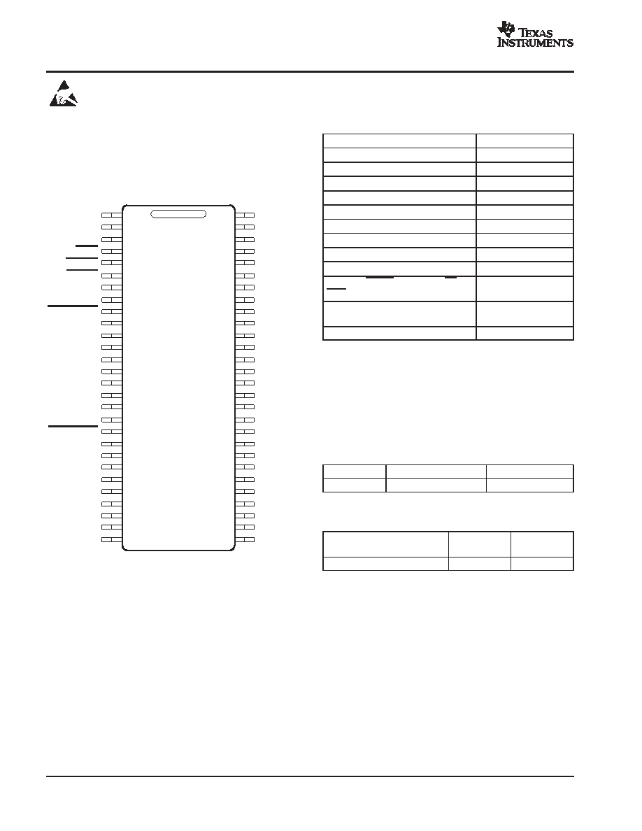
GENERAL INFORMATION
Terminal Assignment
The TAS5112 is offered in a thermally enhanced 56-pin
TSSOP DFD (thermal pad is on the top), shown as follows.
1
2
3
4
5
6
7
8
9
10
11
12
13
14
15
16
17
18
19
20
21
22
23
24
25
26
27
28
56
55
54
53
52
51
50
49
48
47
46
45
44
43
42
41
40
39
38
37
36
35
34
33
32
31
30
29
GND
GREG
OTW
SD_CD
SD_AB
PWM_DP
PWM_DM
RESET_CD
PWM_CM
PWM_CP
DREG_RTN
M3
M2
M1
DREG
PWM_BP
PWM_BM
RESET_AB
PWM_AM
PWM_AP
GND
DGND
GND
DVDD
GREG
GND
GVDD
BST_D
PVDD_D
OUT_D
GND
OUT_C
PVDD_C
BST_C
BST_B
PVDD_B
OUT_B
GND
OUT_A
PVDD_A
BST_A
GVDD
GND
DFD PACKAGE
(TOP VIEW)
ABSOLUTE MAXIMUM RATINGS
over operating free-air temperature range unless otherwise noted(1)
TAS5112
UNITS
DVDD TO DGND
–0.3 V to 4.2 V
GVDD TO GND
33.5 V
PVDD_X TO GND (dc voltage)
33.5 V
PVDD_X TO GND (spike voltage(2))
48 V
OUT_X TO GND (dc voltage)
33.5 V
OUT_X TO GND (spike voltage(2))
48 V
BST_X TO GND (dc voltage)
48 V
BST_X TO GND (spike voltage(2))
53 V
GREG TO GND (3)
14.2 V
PWM_XP, RESET, M1, M2, M3, SD,
OTW
–0.3 V to DVDD + 0.3 V
Maximum operating junction
temperature, TJ
–40
°C to 150°C
Storage temperature
–40
°C to 125°C
(1) Stresses beyond those listed under “absolute maximum ratings”
may cause permanent damage to the device. These are stress
ratings only, and functional operation of the device at these or any
other conditions beyond those indicated under “recommended
operating conditions” is not implied. Exposure to absolute-
maximum-rated conditions for extended periods may affect device
reliability.
(2) The duration of voltage spike should be less than 100 ns.
(3) GREG is treated as an input when the GREG pin is overdriven by
GVDD of 12 V.
ORDERING INFORMATION
TA
PACKAGE
DESCRIPTION
0
°C to 70°C
TAS5112DFD
56-pin small TSSOP
(1) For the most current specification and package information, refer to
our Web site at www.ti.com.
PACKAGE DISSIPATION RATINGS
PACKAGE
RθJC
(
°C/W)
RθJA
(
°C/W)
56-pin DAD TSSOP
1.14
See Note 1
(1) The TAS5112 package is thermally enhanced for conductive
cooling using an exposed metal pad area. It is impractical to use the
device with the pad exposed to ambient air as the only heat sinking
of the device.
For this reason, RθJA, a system parameter that characterizes the
thermal treatment, is provided in the Application Information section
of the data sheet. An example and discussion of typical system
RθJA values are provided in the Thermal Information section. This
example provides additional information regarding the power
dissipation ratings. This example should be used as a reference to
calculate the heat dissipation ratings for a specific application. TI
application engineering provides technical support to design
heatsinks if needed.
相关PDF资料 |
PDF描述 |
|---|---|
| TAS5121DKDE4 | 100 W, 2 CHANNEL, AUDIO AMPLIFIER, PDSO36 |
| TAS5121DKDRE4 | 100 W, 2 CHANNEL, AUDIO AMPLIFIER, PDSO36 |
| TAS5121DKDR | 100 W, 2 CHANNEL, AUDIO AMPLIFIER, PDSO36 |
| TAS5121DKD | 100 W, 2 CHANNEL, AUDIO AMPLIFIER, PDSO36 |
| TAS5121IDKDE4 | 100 W, 2 CHANNEL, AUDIO AMPLIFIER, PDSO36 |
相关代理商/技术参数 |
参数描述 |
|---|---|
| TAS5112DFDR | 功能描述:音频放大器 Dig Amp Stereo Power Stage RoHS:否 制造商:STMicroelectronics 产品:General Purpose Audio Amplifiers 输出类型:Digital 输出功率: THD + 噪声: 工作电源电压:3.3 V 电源电流: 最大功率耗散: 最大工作温度: 安装风格:SMD/SMT 封装 / 箱体:TQFP-64 封装:Reel |
| TAS5112DFDRG4 | 功能描述:音频放大器 Dig Amp Stereo Power Stage RoHS:否 制造商:STMicroelectronics 产品:General Purpose Audio Amplifiers 输出类型:Digital 输出功率: THD + 噪声: 工作电源电压:3.3 V 电源电流: 最大功率耗散: 最大工作温度: 安装风格:SMD/SMT 封装 / 箱体:TQFP-64 封装:Reel |
| TAS5121 | 制造商:TI 制造商全称:Texas Instruments 功能描述:DIGITAL AMPLIFIER POWER STAGE |
| TAS5121_07 | 制造商:TI 制造商全称:Texas Instruments 功能描述:DIGITAL AMPLIIFIER POWER STAGE |
| TAS5121A | 制造商:TI 制造商全称:Texas Instruments 功能描述:DIGITAL AMPLIFIER POWER STAGE |
发布紧急采购,3分钟左右您将得到回复。