- 您现在的位置:买卖IC网 > PDF目录98161 > TAS5121DKDE4 (TEXAS INSTRUMENTS INC) 100 W, 2 CHANNEL, AUDIO AMPLIFIER, PDSO36 PDF资料下载
参数资料
| 型号: | TAS5121DKDE4 |
| 厂商: | TEXAS INSTRUMENTS INC |
| 元件分类: | 音频/视频放大 |
| 英文描述: | 100 W, 2 CHANNEL, AUDIO AMPLIFIER, PDSO36 |
| 封装: | GREEN, PLASTIC, HSSOP-36 |
| 文件页数: | 5/21页 |
| 文件大小: | 591K |
| 代理商: | TAS5121DKDE4 |
TAS5121
SLES086A NOVEMBER 2003 REVISED MARCH 2004
www.ti.com
13
Table 3. Output Mode Selection
M3
OUTPUT MODE
0
Bridge-tied load output stage (BTL)
1
Reserved
APPLICATION INFORMATION
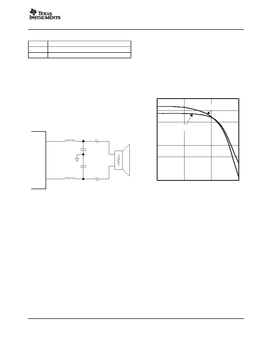
DEMODULATION FILTER DESIGN
The TAS5121 amplifier outputs are driven by high-current
DMOS transistors in an H-bridge configuration. These
transistors are either off or fully on.
The result is a square-wave output signal with a duty cycle
that is proportional to the amplitude of the audio signal. It
is recommended that a second-order LC filter be used to
recover the audio signal.
Output A
C1
TAS5121
L
Output B
L
C2
R(Load)
Figure 10. Demodulation Filter
The main purpose of the demodulation filter is to attenuate
the high-frequency components of the output signals that
are out of the audio band.
Design of the demodulation filter affects the audio
performance of the power amplifier significantly. As a
result, to ensure proper operation of the overcurrent (OC)
protection
circuit
and
meet
the
device
THD+N
specifications, the selection of the inductors used in the
output filter must be considered according to the following.
The rule is that the inductance should remain stable within
the range of peak current seen at maximum output power
and deliver approximately 5
H of inductance at 15 A.
If this rule is observed, the TAS5121 should not have
distortion issues due to the output inductors. This prevents
device damage due to overcurrent conditions because of
inductor saturation in the output filter.
Another parameter to be considered is the idle current loss
in the inductor. This can be measured or specified as
inductor dissipation (D). The target specification for
dissipation is less than 0.05. If this specification is not met,
idle current increases.
In general, 10-
H inductors suffice for most applications.
The frequency response of the amplifier is slightly altered
by the change in output load resistance; however, unless
tight control of frequency response is necessary (better
than 0.5 dB), it is not necessary to deviate from 10
H.
The graphs in Figure 11 display the inductance vs current
characteristics of two inductors that are suggested for use
with the TAS5121.
Figure 11. Inductance Saturation
I Current A
4
5
6
7
8
9
10
11
0
5
10
15
L
Inductance
H
INDUCTANCE
vs
CURRENT
DBF1310A
DASL983XX1023
The selection of the capacitors that are placed from the
output of each inductor to ground is simple. To complete
the output filter, use a 1-
F capacitor with a voltage rating
at least twice the voltage applied to the output stage
(PVDD_x).
This capacitor should be a good quality polyester
dielectric.
THERMAL INFORMATION
The following is provided as an example.
The thermally enhanced package provided with the
TAS5121 are designed to be interfaced directly to
heatsinks using a thermal interface compound (for
example, Wakefield Engineering type 126 thermal
grease.) The heatsink then absorbs heat from the ICs and
transfers it to the ambient air. If the heatsink is carefully
designed, this process can reach equilibrium and heat can
be continually removed from the ICs without device
overtemperature shutdown. Because of the efficiency of
the TAS5121, heatsinks are smaller than those required
for linear amplifiers of equivalent performance.
相关PDF资料 |
PDF描述 |
|---|---|
| TAS5121DKDRE4 | 100 W, 2 CHANNEL, AUDIO AMPLIFIER, PDSO36 |
| TAS5121DKDR | 100 W, 2 CHANNEL, AUDIO AMPLIFIER, PDSO36 |
| TAS5121DKD | 100 W, 2 CHANNEL, AUDIO AMPLIFIER, PDSO36 |
| TAS5121IDKDE4 | 100 W, 2 CHANNEL, AUDIO AMPLIFIER, PDSO36 |
| TAS5121IDKDRE4 | 100 W, 2 CHANNEL, AUDIO AMPLIFIER, PDSO36 |
相关代理商/技术参数 |
参数描述 |
|---|---|
| TAS5121DKDR | 功能描述:音频放大器 TAS5121 Digital Amp Power Stage RoHS:否 制造商:STMicroelectronics 产品:General Purpose Audio Amplifiers 输出类型:Digital 输出功率: THD + 噪声: 工作电源电压:3.3 V 电源电流: 最大功率耗散: 最大工作温度: 安装风格:SMD/SMT 封装 / 箱体:TQFP-64 封装:Reel |
| TAS5121DKDRE4 | 功能描述:音频放大器 TAS5121 Digital Amp Power Stage RoHS:否 制造商:STMicroelectronics 产品:General Purpose Audio Amplifiers 输出类型:Digital 输出功率: THD + 噪声: 工作电源电压:3.3 V 电源电流: 最大功率耗散: 最大工作温度: 安装风格:SMD/SMT 封装 / 箱体:TQFP-64 封装:Reel |
| TAS5121I | 制造商:TI 制造商全称:Texas Instruments 功能描述:DIGITAL AMPLIIFIER POWER STAGE |
| TAS5121IDKD | 功能描述:音频放大器 Digital Amplifier Power Stage RoHS:否 制造商:STMicroelectronics 产品:General Purpose Audio Amplifiers 输出类型:Digital 输出功率: THD + 噪声: 工作电源电压:3.3 V 电源电流: 最大功率耗散: 最大工作温度: 安装风格:SMD/SMT 封装 / 箱体:TQFP-64 封装:Reel |
| TAS5121IDKDE4 | 功能描述:音频放大器 Digital Amplifier Power Stage RoHS:否 制造商:STMicroelectronics 产品:General Purpose Audio Amplifiers 输出类型:Digital 输出功率: THD + 噪声: 工作电源电压:3.3 V 电源电流: 最大功率耗散: 最大工作温度: 安装风格:SMD/SMT 封装 / 箱体:TQFP-64 封装:Reel |
发布紧急采购,3分钟左右您将得到回复。