- 您现在的位置:买卖IC网 > PDF目录196350 > TC1073-2.85VCH713 2.85 V FIXED POSITIVE LDO REGULATOR, 0.25 V DROPOUT, PDSO6 PDF资料下载
参数资料
| 型号: | TC1073-2.85VCH713 |
| 元件分类: | 固定正电压单路输出LDO稳压器 |
| 英文描述: | 2.85 V FIXED POSITIVE LDO REGULATOR, 0.25 V DROPOUT, PDSO6 |
| 封装: | PLASTIC, SOT-23, 6 PIN |
| 文件页数: | 5/22页 |
| 文件大小: | 713K |
| 代理商: | TC1073-2.85VCH713 |
2007 Microchip Technology Inc.
DS21354D-page 13
TC1072/TC1073
5.0
THERMAL CONSIDERATIONS
5.1
Thermal Shutdown
Integrated thermal protection circuitry shuts the
regulator off when die temperature exceeds 160°C.
The regulator remains off until the die temperature
drops to approximately 150°C.
5.2
Power Dissipation
The amount of power the regulator dissipates is
primarily a function of input and output voltage, and
output current. The following equation is used to
calculate worst-case actual power dissipation:
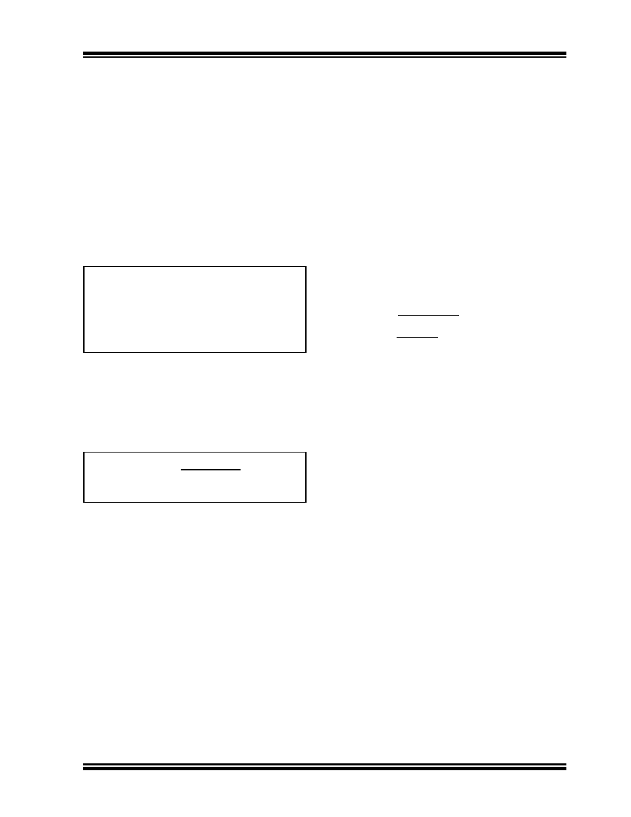
EQUATION 5-1:
The
maximum
allowable
power
dissipation
(Equation 5-2) is a function of the maximum ambient
temperature (TAMAX), the maximum allowable die tem-
perature (TJMAX) and the thermal resistance from junc-
tion-to-air (
θJA). The 6-Pin SOT-23 package has a θJA
of approximately 220°C/Watt.
EQUATION 5-2:
Equation 5-1 can be used in conjunction with
Equation 5-2 to ensure regulator thermal operation is
within limits. For example:
Given:
VINMAX
= 3.0V ±5%
VOUTMIN
= 2.7V – 2.5%
ILOADMAX
= 40 mA
TJMAX
= 125°C
TAMAX
= 55°C
Find:
1. Actual power dissipation
2. Maximum allowable dissipation
Actual power dissipation:
PD ≈ (VINMAX – VOUTMIN)ILOADMAX
= [(3.0 x 1.05) – (2.7 x 0.975)] x 40 x 10–3
= 20.7 mW
Maximum allowable power dissipation:
In this example, the TC1072 dissipates a maximum of
20.7 mW; below the allowable limit of 318 mW. In a
similar manner, Equation 5-1 and Equation 5-2 can be
used to calculate maximum current and/or input
voltage limits.
5.3
Layout Considerations
The primary path of heat conduction out of the package
is via the package leads. Therefore, layouts having a
ground plane, wide traces at the pads, and wide power
supply bus lines combine to lower
θJA and therefore
increase the maximum allowable power dissipation
limit.
Where:
PD ≈ (VINMAX – VOUTMIN)ILOADMAX
PD
VINMAX
VOUTMIN
ILOADMAX
= Worst-case actual power dissipation
= Minimum regulator output voltage
= Maximum output (load) current
= Maximum voltage on VIN
PDMAX = (TJMAX – TAMAX)
θJA
where all terms are previously defined.
PDMAX = (TJMAX – TAMAX)
θJA
= (125 – 55)
220
= 318 mW
相关PDF资料 |
PDF描述 |
|---|---|
| TC1073-2.7VCH713 | 2.7 V FIXED POSITIVE LDO REGULATOR, 0.25 V DROPOUT, PDSO6 |
| TC1221ECHRT | SWITCHED CAPACITOR CONVERTER, 169 kHz SWITCHING FREQ-MAX, PDSO6 |
| TC211 | SPECIALTY ANALOG CIRCUIT, CDIP6 |
| TC4066BF(EL) | QUAD 1-CHANNEL, SGL POLE SGL THROW SWITCH, PDSO14 |
| TC47H050E-FREQ | TCXO, CLOCK, 10 MHz - 60 MHz, HCMOS/TTL OUTPUT |
相关代理商/技术参数 |
参数描述 |
|---|---|
| TC1073-28VCH | 制造商:MICROCHIP 制造商全称:Microchip Technology 功能描述:50mA and 100mA CMOS LDOs with Shutdown, ERROR Output and VREF Bypass |
| TC1073-3.0VCH713 | 功能描述:低压差稳压器 - LDO .1mA w/Shtdn & Error 3.0V RoHS:否 制造商:Texas Instruments 最大输入电压:36 V 输出电压:1.4 V to 20.5 V 回动电压(最大值):307 mV 输出电流:1 A 负载调节:0.3 % 输出端数量: 输出类型:Fixed 最大工作温度:+ 125 C 安装风格:SMD/SMT 封装 / 箱体:VQFN-20 |
| TC10733.0VCT713 | 制造商:MICROCHIP 制造商全称:Microchip Technology 功能描述:50mA and 100mA CMOS LDOs with Shutdown, ERROR Output and VREF Bypass |
| TC1073-3.3VCH713 | 功能描述:低压差稳压器 - LDO .1mA w/Shtdn & Error 3.3V RoHS:否 制造商:Texas Instruments 最大输入电压:36 V 输出电压:1.4 V to 20.5 V 回动电压(最大值):307 mV 输出电流:1 A 负载调节:0.3 % 输出端数量: 输出类型:Fixed 最大工作温度:+ 125 C 安装风格:SMD/SMT 封装 / 箱体:VQFN-20 |
| TC10733.3VCT713 | 制造商:MICROCHIP 制造商全称:Microchip Technology 功能描述:50mA and 100mA CMOS LDOs with Shutdown, ERROR Output and VREF Bypass |
发布紧急采购,3分钟左右您将得到回复。