- 您现在的位置:买卖IC网 > PDF目录98167 > TC115501ECT 0.4 A SWITCHING REGULATOR, 115 kHz SWITCHING FREQ-MAX, PDSO5 PDF资料下载
参数资料
| 型号: | TC115501ECT |
| 元件分类: | 稳压器 |
| 英文描述: | 0.4 A SWITCHING REGULATOR, 115 kHz SWITCHING FREQ-MAX, PDSO5 |
| 封装: | SOT-89, 5 PIN |
| 文件页数: | 7/14页 |
| 文件大小: | 468K |
| 代理商: | TC115501ECT |
TC115
DS21361B-page 2
2002 Microchip Technology Inc.
1.0
ELECTRICAL
CHARACTERISTICS
Absolute Maximum Ratings*
Power Supply Voltage (PS) .................................... 12V
Power Dissipation.............................................500mW
LX Sink Current ............................................ 400mA pk
SHDN Input Voltage ............................................... 12V
Operating Temperature Range............. -40°C to +85°C
Storage Temperature Range .............. -40°C to +125°C
*Stresses above those listed under "Absolute Maximum
Ratings" may cause permanent damage to the device. These
are stress ratings only and functional operation of the device
at these or any other conditions above those indicated in the
operation sections of the specifications is not implied.
Exposure to Absolute Maximum Rating conditions for
extended periods may affect device reliability.
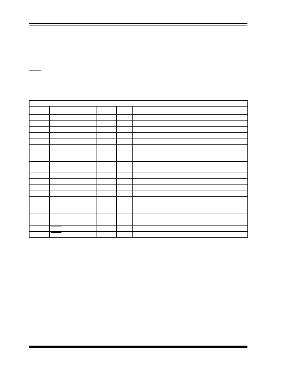
TC115 ELECTRICAL SPECIFICATIONS
Electrical Characteristics: VOUT =5V, TA = 25°C, unless otherwise noted. Circuit configuration per Figure 4-1.
Symbol
Parameter
Min
Typ
Max
Units
Test Conditions
VIN
Operating Supply Voltage
0.9
—
10.0
V
Note 5
VSTART
Start-Up Supply Voltage
—
0.9
V
IOUT =1mA
ILXMAX
LX Maximum Sink Current
—
350
mA
fLIM
LX Limit Frequency
—
200
—
kHz
VLX =VLXLIM
VLXLIM
LX Limit Voltage
0.7
—
1.3
V
Note 2
IDD
No Load Supply Current
—
13
26
AIOUT =0, VIN =VOUT x 0.8 (Note3)
ICC
Boost Mode Supply Current
—
80
135
A
No external components,
VIN =(0.95 x VOUT) applied to PS (or VDD) input
ISTBY
Standby Supply Current
—
9
17
A
No external components,
VIN =(1.1x VOUT) applied to PS (or VDD) input
ISD
Shutdown Supply Current
—
0.5
A
SHDN =0V
fOSC
Oscillator Frequency
85
100
115
kHz
Note 2, Note 4
VOUT
Output Voltage
VR x0.975
VR
VR x1.025
V
VIN =2.2V minimum (Note1)
RSWON
LX Output ON Resistance
—
1.4
2.4
VLX =0.4V
PFMDUTY Duty Cycle
(PFM Operating Mode)
10
17
25
%
No external components.
MAXDUTY Maximum Duty Cycle
80
87
92
%
Note 4
tSS
Soft Start Time
4
10
20
msec
η
Efficiency
—
85
—
%
VIH
SHDN Input Logic High
0.75
—
V
VIL
SHDN Input Logic Low
—
0.20
V
Note
1:
VR is the nominal factory-programmed output voltage setting.
2:
VLXLIM is the voltage on the LX pin (with internal switch ON) that will cause the oscillator to run at twice nominal frequency in to limit the
switch current through the internal N-channel switching transistor.
3:
Measured with D1 = MA735 (reverse current < 1
A at a reverse voltage of 10V).
4:
With TC115 operating in PWM mode.
5:
See Section 3.4 “Behavior When VIN is Greater Than the Factory-Programmed VOUT Setting”.
相关PDF资料 |
PDF描述 |
|---|---|
| TC115301ECT | 0.4 A SWITCHING REGULATOR, 115 kHz SWITCHING FREQ-MAX, PDSO5 |
| TC1219ECHTR | SWITCHED CAPACITOR CONVERTER, 20 kHz SWITCHING FREQ-MAX, PDSO6 |
| TC126301ECT | 0.4 A SWITCHING REGULATOR, 115 kHz SWITCHING FREQ-MAX, PDSO5 |
| TC126331ECT | 0.4 A SWITCHING REGULATOR, 115 kHz SWITCHING FREQ-MAX, PDSO5 |
| TC1275-20ENBTR | 1-CHANNEL POWER SUPPLY SUPPORT CKT, PDSO3 |
相关代理商/技术参数 |
参数描述 |
|---|---|
| TC115501EMTTR | 功能描述:开关变换器、稳压器与控制器 PFM/PWM Step-Up RoHS:否 制造商:Texas Instruments 输出电压:1.2 V to 10 V 输出电流:300 mA 输出功率: 输入电压:3 V to 17 V 开关频率:1 MHz 工作温度范围: 安装风格:SMD/SMT 封装 / 箱体:WSON-8 封装:Reel |
| TC115A | 制造商:Thomas & Betts 功能描述:1 1/2" Compression Connector, Steel-Zinc Plated, Concrete tight 制造商:Thomas & Betts 功能描述:Fittings Connector 1.5inch Steel |
| TC115A-RT | 制造商:Thomas & Betts 功能描述:Fittings Connector 1.5inch Male Steel |
| TC115EV | 功能描述:电源管理IC开发工具 PFM/PWM Boost Conv EVAL BRD RoHS:否 制造商:Maxim Integrated 产品:Evaluation Kits 类型:Battery Management 工具用于评估:MAX17710GB 输入电压: 输出电压:1.8 V |
| TC115-PB-B | 制造商:Carling Technologies 功能描述:T-SERIES ROCKER SWITCH - Bulk |
发布紧急采购,3分钟左右您将得到回复。