- 您现在的位置:买卖IC网 > PDF目录136952 > TC120333EHATR 0.7 A SWITCHING REGULATOR, 345 kHz SWITCHING FREQ-MAX, PDSO8 PDF资料下载
参数资料
| 型号: | TC120333EHATR |
| 元件分类: | 稳压器 |
| 英文描述: | 0.7 A SWITCHING REGULATOR, 345 kHz SWITCHING FREQ-MAX, PDSO8 |
| 封装: | SOP, 8 PIN |
| 文件页数: | 6/10页 |
| 文件大小: | 80K |
| 代理商: | TC120333EHATR |
5
TC120
PWM/PFM STEP-DOWN COMBINATION
REGULATOR/CONTROLLER
TC120-1 7/27/99
recovered to nominal value prior to the expiration of the
protection timer, the TC120 is momentarily shut down by
dedicated, internal circuitry. Immediately following this ac-
tion, the soft start sequence is engaged in an attempt to re-
start the TC120. If the output short circuit is removed, normal
operation is automatically restored. If the short circuit is still
present, the timed self-shutdown sequence described above
is repeated.
Operation as a Regulator Controller
External Switching Transistor Selection
EXT is a complimentary output with a maximum ON
resistances of 32
to VDD when high and 26 to ground
when low, at VOUT = 5V. It is designed to directly drive a P-
channel MOSFET (Figure 7). The P-channel MOSFET
selection is determined mainly by the on-resistance, gate-
source threshold and gate charge requirements. Also, the
drain-to-source and gate-to-source breakdown voltage rat-
ings must be greater than VIN(MAX). The total gate charge
specification should be less than 100 nC for best efficiency.
The MOSFET must be capable of handling the required
peak inductor current, and should have a very low on-
resistance at that current. For example, a Si9430 MOSFET
has a drain-to-source rating of –20V, and a typical on-
resistance rDS(ON) of 0.07 at 2A, with VGS = –4.5V. (EXTW
(Figure 8) may be gated with external circuitry to add
blanking, or as an auxiliary timing signal.) Table A lists
suppliers of external components recommended for use
with the TC120.
Board Layout Guidelines
As with all inductive switching regulators, the TC120
generates fast switching waveforms, which radiate noise.
Interconnecting lead lengths should be minimized to keep
stray capacitance, trace resistance and radiated noise as
low as possible. In addition, the GND pin, input bypass
capacitor and output filter capacitor ground leads should be
connected to a single point. The input capacitor should be
placed as close to power and ground pins of the TC120 as
possible. The length of the EXT trace must also be kept as
short as possible.
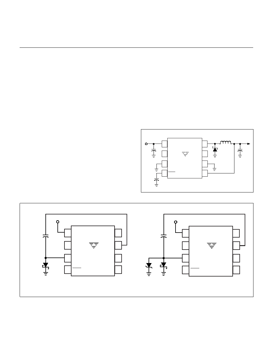
Figure 2. TC120 Typical Application
Figure 3. TC120 with Added Components for Improved Efficiency at High Output Currents
TC120xx03
VIN
EXTW
CPC
SHDN/SS
LX
EXT
GND
SENSE
CIN
D1
L1
VOUT
VIN
COUT
CSS
4.7 nF
TC120xx03
VIN
EXTW
CPC
SHDN/SS
LX
EXT
GND
SENSE
D1
IN5817
a) For VIN ≤ 5V
CP
2200 pF
Ceramic
TC120xx03
VIN
EXTW
CPC
SHDN/SS
LX
EXT
GND
SENSE
D1
IN5817
b) For VIN > 5V
CP
2200 pF
Ceramic
10V
Zener
Diode
VIN ≤ 5V
VIN > 5V
相关PDF资料 |
PDF描述 |
|---|---|
| TA7291P | BRUSH DC MOTOR CONTROLLER, 2 A, PSFM10 |
| TA7291S | BRUSH DC MOTOR CONTROLLER, 1.2 A, PSIP9 |
| TSP2100DBVR | 2-CHANNEL POWER SUPPLY SUPPORT CKT, PDSO5 |
| TL7702BID | 1-CHANNEL POWER SUPPLY SUPPORT CKT, PDSO8 |
| TL431AILP/1H | 1-OUTPUT THREE TERM VOLTAGE REFERENCE, 2.5 V, PBCY3 |
相关代理商/技术参数 |
参数描述 |
|---|---|
| TC120503EHA | 制造商:MICROCHIP 制造商全称:Microchip Technology 功能描述:PWM/PFM Step-Down Combination Regulator/Controller |
| TC120503EHATR | 功能描述:开关变换器、稳压器与控制器 PWM/PFM Step-Down RoHS:否 制造商:Texas Instruments 输出电压:1.2 V to 10 V 输出电流:300 mA 输出功率: 输入电压:3 V to 17 V 开关频率:1 MHz 工作温度范围: 安装风格:SMD/SMT 封装 / 箱体:WSON-8 封装:Reel |
| TC1207D-100M | 制造商:PRODUCTWELL 制造商全称:PRODUCTWELL 功能描述:TOROID INDUCTORS |
| TC1207D-320M | 制造商:PRODUCTWELL 制造商全称:PRODUCTWELL 功能描述:TOROID INDUCTORS |
| TC1210A | 制造商:Thomas & Betts 功能描述:Fittings Connector 4inch Steel |
发布紧急采购,3分钟左右您将得到回复。