- 您现在的位置:买卖IC网 > PDF目录136945 > TC1226EUATR SWITCHED CAPACITOR CONVERTER, 45.5 kHz SWITCHING FREQ-MAX, PDSO8 PDF资料下载
参数资料
| 型号: | TC1226EUATR |
| 元件分类: | 稳压器 |
| 英文描述: | SWITCHED CAPACITOR CONVERTER, 45.5 kHz SWITCHING FREQ-MAX, PDSO8 |
| 封装: | MSOP-8 |
| 文件页数: | 1/9页 |
| 文件大小: | 1189K |
| 代理商: | TC1226EUATR |
TC1225/6/7-1
3/24/00
TC1225
TC1226
TC1227
2001 Microchip Technology Inc.
DS21369A
Inverting Dual (–VIN, –2VIN) Charge Pump Voltage Converters
FEATURES
s
Small 8-Pin MSOP Package
s
Operates from 1.8V to 5.5V
s
Up to 5mA Output Current at –VIN Pin
s
Up to 1mA Output Current at –2VIN Pin
s
–VIN and –2VIN Outputs Available
s
Low Supply Current
.......................................... 120
A (MAX) for TC1225
.......................................... 360
A (MAX) for TC1226
.......................................... 1.5mA (MAX) for TC1227
TYPICAL APPLICATIONS
s
LCD Panel Bias
s
Cellular Phones PA Bias
s
Pagers
s
PDAs, Portable Data loggers
s
Battery Powered Devices
GENERAL DESCRIPTION
The TC1225/1226/1227 are CMOS dual inverting charge
pump voltage converters in 8-Pin MSOP packages. An on-
board oscillator provides the clock, and only four external
capacitors are required for full circuit implementation. Switch-
ing frequencies are 12kHz for the TC1225, 35kHz for the
TC1226, and 125kHz for the TC1227.
These devices provide both a negative voltage inversion
(available at the –VIN output) and a negative doubling
voltage inversion (available at the –2 VIN output), with a low
output impedance capable of providing output currents up to
5mA for the –VIN output and 1mA for the –2VIN output. The
input voltage can range from +1.8V to +5.5V.
ORDERING INFORMATION
Part No.
Package Osc Freq (kHz) Temp Range
TC1225EUA
8-Pin MSOP
12
–40
°C to +85°C
TC1226EUA
8-Pin MSOP
35
–40
°C to +85°C
TC1227EUA
8-Pin MSOP
125
–40
°C to +85°C
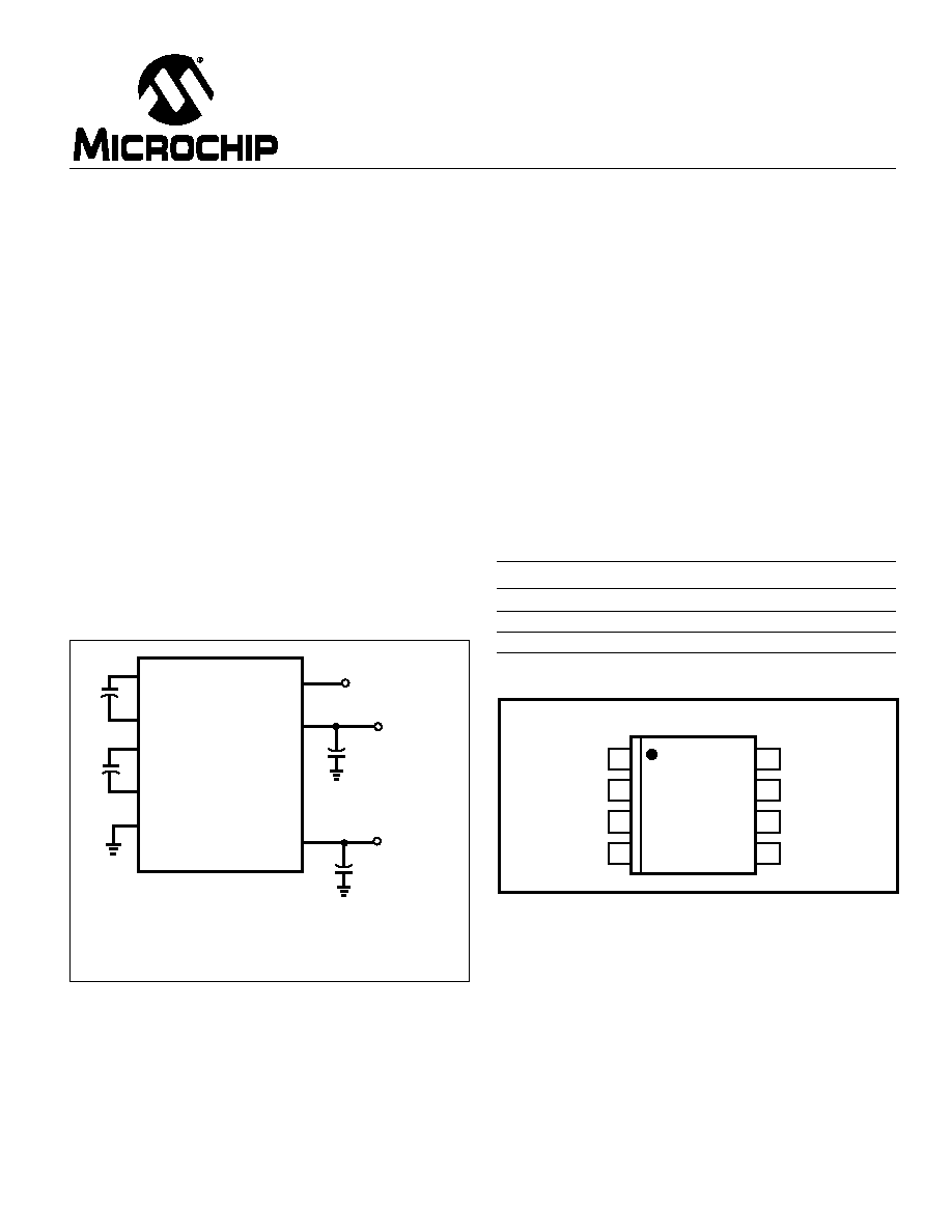
TYPICAL OPERATING CIRCUIT
C1+
C2+
VIN
–VIN
C1–
C2
C2–
C1
TC1225
TC1226
TC1227
COUT1
–2 VIN
+
–
+
– COUT2
OUTPUT 1
OUTPUT 2
INPUT
GND
PIN CONFIGURATION
1
2
3
4
8
7
6
5
TC1225
TC1226
TC1227
–2VIN
–VIN
VIN
C2–
GND
C1–
C1+
C2+
8-Pin MSOP
Notes:
1) C1 and COUT1 must have a voltage rating greater
than or equal to VIN
2) C2 and COUT2 must have a voltage rating greater
than or equal to 2VIN
相关PDF资料 |
PDF描述 |
|---|---|
| TPIC9201PWPRG4 | 1-CHANNEL POWER SUPPLY SUPPORT CKT, PDSO20 |
| TRU050GACGA24.576 | PHASE LOCKED LOOP, CDSO16 |
| TRU050GACGB12.624 | PHASE LOCKED LOOP, CDSO16 |
| TRU050GACNB12 | PHASE LOCKED LOOP, CDSO16 |
| TRU050GALGB18.432 | PHASE LOCKED LOOP, CDSO16 |
相关代理商/技术参数 |
参数描述 |
|---|---|
| TC1227 | 制造商:MICROCHIP 制造商全称:Microchip Technology 功能描述:Inverting Dual (-VIN, -2VIN) Charge Pump Voltage Converters |
| TC1227EUA | 制造商:MICROCHIP 制造商全称:Microchip Technology 功能描述:Inverting Dual (-VIN, -2VIN) Charge Pump Voltage Converters |
| TC122A | 制造商:Thomas & Betts 功能描述:Fittings Connector 0.75inch Steel |
| TC122A-FA | 制造商:Thomas & Betts 功能描述:Fittings Connector 0.75inch Steel |
| TC122-JR-070RL | 制造商:Yageo Corporation 功能描述:RESISTOR ARRAY ARC321 0R 制造商:Yageo / Phycomp 功能描述:RESISTOR ARRAY, ARC321, 0R |
发布紧急采购,3分钟左右您将得到回复。