- 您现在的位置:买卖IC网 > PDF目录383894 > TC1303A-AS1EMFTR (Microchip Technology Inc.) 500 mA Synchronous Buck Regulator, + 300 mA LDO with Power-Good Output PDF资料下载
参数资料
| 型号: | TC1303A-AS1EMFTR |
| 厂商: | Microchip Technology Inc. |
| 英文描述: | 500 mA Synchronous Buck Regulator, + 300 mA LDO with Power-Good Output |
| 中文描述: | 500毫安同步降压稳压器,300 mA的LDO具有电源就绪输出 |
| 文件页数: | 6/36页 |
| 文件大小: | 463K |
| 代理商: | TC1303A-AS1EMFTR |
第1页第2页第3页第4页第5页当前第6页第7页第8页第9页第10页第11页第12页第13页第14页第15页第16页第17页第18页第19页第20页第21页第22页第23页第24页第25页第26页第27页第28页第29页第30页第31页第32页第33页第34页第35页第36页
TC1303A/TC1303B/TC1303C/TC1304
DS21949B-page 6
2005 Microchip Technology Inc.
1.0
ELECTRICAL
CHARACTERISTICS
Absolute Maximum Ratings
V
IN
- A
GND
......................................................................6.0V
All Other I/O .............................. (A
GND
- 0.3V) to (V
IN
+ 0.3V)
L
X
to P
GND
.............................................. -0.3V to (V
IN
+ 0.3V)
P
GND
to A
GND
...................................................-0.3V to +0.3V
Output Short Circuit Current .................................Continuous
Power Dissipation (
Note 7
)..........................Internally Limited
Storage temperature .....................................-65°C to +150°C
Ambient Temp. with Power Applied.................-40°C to +85°C
Operating Junction Temperature...................-40°C to +125°C
ESD protection on all pins (HBM)
.......................................
3 kV
Notice:
Stresses above those listed under “Maximum
Ratings” may cause permanent damage to the device. This is
a stress rating only and functional operation of the device at
those or any other conditions above those indicated in the
operational listings of this specification is not implied.
Exposure to maximum rating conditions for extended periods
may affect device reliability.
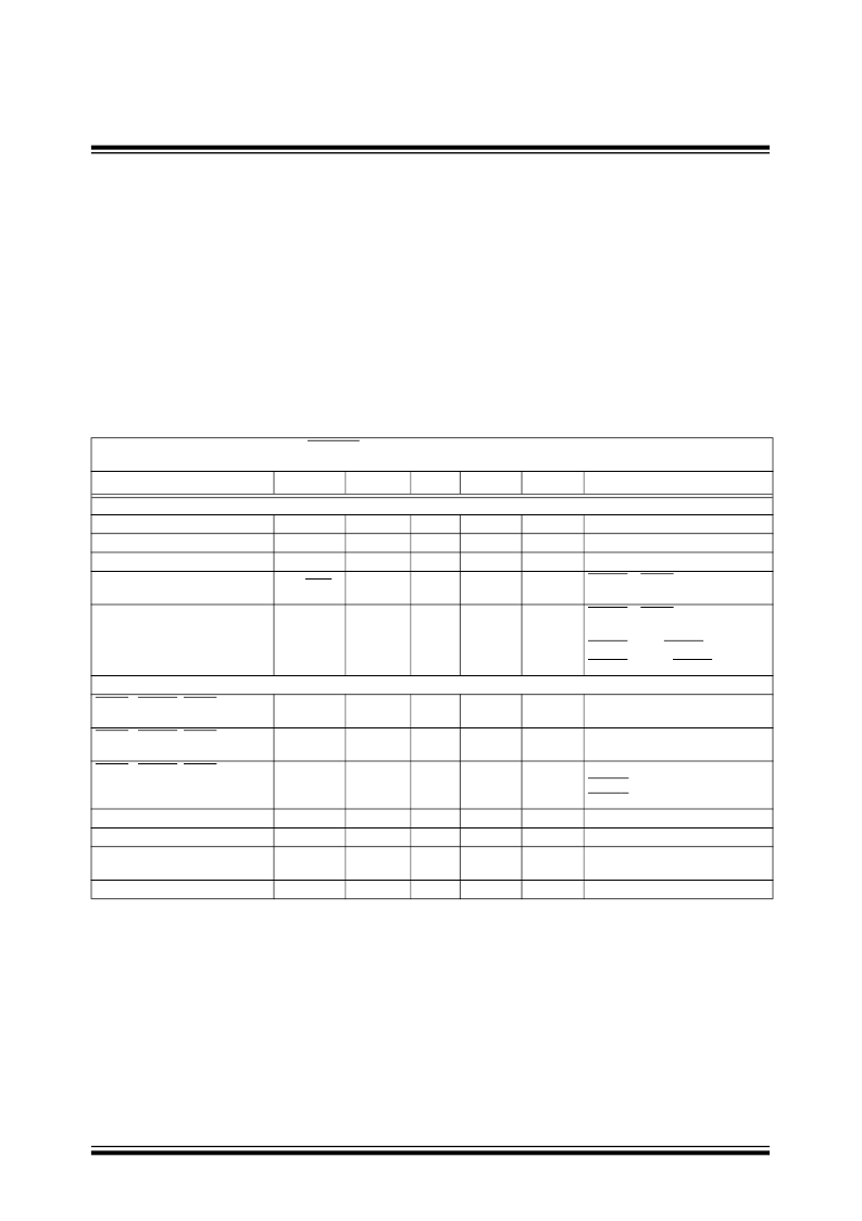
DC CHARACTERISTICS
Electrical Characteristics:
V
IN1
=V
IN2
= SHDN1,2 = 3.6V, C
OUT1
= C
IN
= 4.7 μF, C
OUT2
= 1μF, L
= 4.7 μH, V
OUT1
(ADJ) = 1.8V,
I
OUT1
= 100 ma, I
OUT2
= 0.1 mA T
A
= +25°C.
Boldface
specifications apply over the T
A
range of
-40°C to +85°C
.
Parameters
Sym
Min
Typ
Max
Units
Conditions
Input/Output Characteristics
Input Voltage
Maximum Output Current
Maximum Output Current
Shutdown Current
Combined V
IN1
and V
IN2
Current
TC1303A,B
Operating I
Q
TC1303C
,
TC1304
Operating I
Q
Synchronous Buck I
Q
LDO I
Q
Shutdown/UVLO/Thermal Shutdown Characteristics
SHDN1,SHDN2, SHDN (
TC1304
)
Logic Input Voltage Low
SHDN1,SHDN2, SHDN (
TC1304
)
Logic Input Voltage High
SHDN1,SHDN2, SHDN (
TC1304
)
Input Leakage Current
V
IN
2.7
500
300
—
—
—
—
0.05
5.5
—
—
1
V
Note 1
,
Note 2, Note 8
Note 1
Note 1
SHDN1 = SHDN2 = GND
I
OUT1_MAX
I
OUT2_MAX
I
IN_SHDN
mA
mA
μA
I
Q
I
Q
—
65.0
70.1
38
46
110
110
—
—
μA
SHDN1 = SHDN2 = V
IN2
I
OUT1
= 0 mA, I
OUT2
= 0 mA
SHDN1 = V
IN
, SHDN2 = GND
SHDN1 = GND, SHDN2 = V
IN2
—
—
μA
μA
V
IL
—
—
15
%V
IN
V
IN1
=V
IN2
= 2.7V to 5.5V
V
IH
45
—
—
%V
IN
V
IN1
=V
IN2
= 2.7V to 5.5V
I
IN
-1.0
±0.01
1.0
μA
V
IN1
=V
IN2
= 2.7V to 5.5V
SHDNX = GND
SHDNY = V
IN
Note 6
,
Note 7
Thermal Shutdown
Thermal Shutdown Hysteresis
Undervoltage Lockout
(V
OUT1
and V
OUT2
)
Undervoltage Lockout Hysteresis
Note
1:
The Minimum V
IN
has to meet two conditions: V
IN
≥
2.7V and V
IN
≥
V
RX
+ V
DROPOUT,
V
RX
= V
R1
or V
R2
.
2:
V
RX
is the regulator output voltage setting.
3:
TCV
OUT2
= ((V
OUT2max
– V
OUT2min
) * 10
6
)/(V
OUT2
* D
T
).
4:
Regulation is measured at a constant junction temperature using low duty-cycle pulse testing. Load regulation is tested
over a load range from 0.1 mA to the maximum specified output current.
5:
Dropout voltage is defined as the input-to-output voltage differential at which the output voltage drops 2% below its
nominal value measured at a 1V differential.
6:
The maximum allowable power dissipation is a function of ambient temperature, the maximum allowable junction
temperature and the thermal resistance from junction to air. (i.e. T
A
, T
J
,
θ
JA
). Exceeding the maximum allowable power
dissipation causes the device to initiate thermal shutdown.
7:
The integrated MOSFET switches have an integral diode from the L
X
pin to V
IN
, and from L
X
to P
GND
. In cases where
these diodes are forward-biased, the package power dissipation limits must be adhered to. Thermal protection is not
able to limit the junction temperature for these cases.
8:
V
IN1
and V
IN2
are supplied by the same input source.
T
SHD
T
SHD-HYS
UVLO
—
—
2.4
165
10
2.55
—
—
2.7
°C
°C
V
V
IN1
Falling
UVLO
-
HYS
—
200
—
mV
相关PDF资料 |
PDF描述 |
|---|---|
| TC1303A-AS1EUN | 500 mA Synchronous Buck Regulator, + 300 mA LDO with Power-Good Output |
| TC1303B-AB2EMFTR | 500 mA Synchronous Buck Regulator, + 300 mA LDO with Power-Good Output |
| TC1303B-AB2EUN | 500 mA Synchronous Buck Regulator, + 300 mA LDO with Power-Good Output |
| TC1303B-AB2EUNTR | 500 mA Synchronous Buck Regulator, + 300 mA LDO with Power-Good Output |
| TC1303B-AB3EMF | 500 mA Synchronous Buck Regulator, + 300 mA LDO with Power-Good Output |
相关代理商/技术参数 |
参数描述 |
|---|---|
| TC1303A-AS1EUN | 制造商:MICROCHIP 制造商全称:Microchip Technology 功能描述:500 mA Synchronous Buck Regulator, + 300 mA LDO with Power-Good Output |
| TC1303A-AS1EUNTR | 制造商:MICROCHIP 制造商全称:Microchip Technology 功能描述:500 mA Synchronous Buck Regulator, + 300 mA LDO with Power-Good Output |
| TC1303A-AS2EMF | 制造商:MICROCHIP 制造商全称:Microchip Technology 功能描述:500 mA Synchronous Buck Regulator, + 300 mA LDO with Power-Good Output |
| TC1303A-AS2EMFTR | 制造商:MICROCHIP 制造商全称:Microchip Technology 功能描述:500 mA Synchronous Buck Regulator, + 300 mA LDO with Power-Good Output |
| TC1303A-AS2EUN | 制造商:MICROCHIP 制造商全称:Microchip Technology 功能描述:500 mA Synchronous Buck Regulator, + 300 mA LDO with Power-Good Output |
发布紧急采购,3分钟左右您将得到回复。