- 您现在的位置:买卖IC网 > PDF目录68276 > TC1304-ZS1EMFTR 0.5 A SWITCHING REGULATOR, 2400 kHz SWITCHING FREQ-MAX, PDSO10 PDF资料下载
参数资料
| 型号: | TC1304-ZS1EMFTR |
| 元件分类: | 稳压器 |
| 英文描述: | 0.5 A SWITCHING REGULATOR, 2400 kHz SWITCHING FREQ-MAX, PDSO10 |
| 封装: | 3 X 3 MM, 0.9 MM HEIGHT, PLASTIC, DFN-10 |
| 文件页数: | 20/38页 |
| 文件大小: | 756K |
| 代理商: | TC1304-ZS1EMFTR |
第1页第2页第3页第4页第5页第6页第7页第8页第9页第10页第11页第12页第13页第14页第15页第16页第17页第18页第19页当前第20页第21页第22页第23页第24页第25页第26页第27页第28页第29页第30页第31页第32页第33页第34页第35页第36页第37页第38页
2008 Microchip Technology Inc.
DS21949C-page 27
TC1303A/TC1303B/TC1303C/TC1304
As an example, for a 3.6V input, 1.8V output with a load
of 400 mA, the efficiency taken from Figure 2-8 is
approximately 84%. The internal power dissipation is
approximately 137 mW.
5.6.2
LDO OUTPUT (VOUT2)
The internal power dissipation within the TC1303/
TC1304 LDO is a function of input voltage, output
voltage and output current. Equation 5-7 can be used
to calculate the internal power dissipation for the LDO.
EQUATION 5-7:
The maximum power dissipation capability for a
package can be calculated given the junction-to-
ambient thermal resistance and the maximum ambient
temperature for the application. The following equation
can be used to determine the package’s maximum
internal power dissipation.
5.6.3
LDO POWER DISSIPATION
EXAMPLE
5.7
PCB Layout Information
Some basic design guidelines should be used when
physically placing the TC1303/TC1304 on a Printed
Circuit Board (PCB). The TC1303/TC1304 has two
ground pins, identified as AGND (analog ground) and
PGND (power ground). By separating grounds, it is
possible to minimize the switching frequency noise on
the LDO output. The first priority, while placing external
components on the board, is the input capacitor (CIN1).
Wiring should be short and wide; the input current for
the TC1303/TC1304 can be as high as 800 mA. The
next priority would be the buck regulator output
capacitor (COUT1) and inductor (L1). All three of these
components are placed near their respective pins to
minimize trace length. The CIN1 and COUT1 capacitor
returns are connected closely together at the PGND
plane. The LDO optional input capacitor (CIN2) and
LDO output capacitor COUT2 are returned to the AGND
plane. The analog ground plane and power ground
plane are connected at one point (shown near L1). All
other signals (SHDN1, SHDN2, feedback in the
adjustable-output case) should be referenced to AGND
and have the AGND plane underneath them.
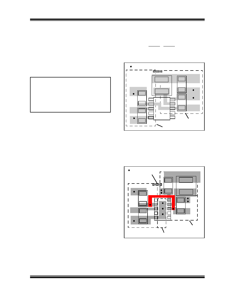
FIGURE 5-1:
Component Placement,
Fixed 10-Pin MSOP.
There will be some difference in layout for the 10-pin
DFN package due to the thermal pad. A typical fixed-
output DFN layout is shown below. For the DFN layout,
the VIN1 to VIN2 connection is routed on the bottom of
the board around the TC1303/TC1304 thermal pad.
FIGURE 5-2:
Component Placement,
Fixed 10-Pin DFN.
Input Voltage
VIN =5V±10%
LDO Output Voltage and Current
VOUT =3.3V
IOUT = 300 mA
Internal Power Dissipation
PLDO(MAX) =(VIN(MAX) – VOUT2(MIN)) x IOUT2(MAX)
PLDO = (5.5V – 0.975 x 3.3V) x 300 mA
PLDO = 684.8 mW
P
LDO
V
IN MAX
)
()
V
OUT2 MIN
()
–
() I
OUT2 MAX
)
()
×
=
Where:
PLDO = LDO Pass device internal power
dissipation
VIN(MAX) = Maximum input voltage
VOUT(MIN) = LDO minimum output voltage
TC1303B
1
2
6
8
7
9
10
5
4
3
+VOUT1
PGND
+VIN1
AGND
+VOUT2
COUT1
CIN2
COUT2
CIN1
PGND Plane
AGND Plane
L1
AGND to PGND
+VIN2
* CIN2 Optional
-
Via
1
2
6
8
7
9
10
5
4
3
+VOUT1
PGND
+VIN1
AGND
+VOUT2
COUT1
CIN2
COUT2
CIN1
PGND Plane
AGND Plane
L1
AGND to PGND
PGND
* CIN2 Optional
+VIN2
TC1303B
- Via
相关PDF资料 |
PDF描述 |
|---|---|
| TC1303A-1C1EUNTR | 0.5 A SWITCHING REGULATOR, 2400 kHz SWITCHING FREQ-MAX, PDSO10 |
| TC1303A-1E1EUNTR | 0.5 A SWITCHING REGULATOR, 2400 kHz SWITCHING FREQ-MAX, PDSO10 |
| TC1303A-1H3EUN | 0.5 A SWITCHING REGULATOR, 2400 kHz SWITCHING FREQ-MAX, PDSO10 |
| TC1303A-1J0EUNTR | 0.5 A SWITCHING REGULATOR, 2400 kHz SWITCHING FREQ-MAX, PDSO10 |
| TC1303A-1J2EUN | 0.5 A SWITCHING REGULATOR, 2400 kHz SWITCHING FREQ-MAX, PDSO10 |
相关代理商/技术参数 |
参数描述 |
|---|---|
| TC1305R-DVUN | 功能描述:低压差稳压器 - LDO Dual LDO w/ Sdn RoHS:否 制造商:Texas Instruments 最大输入电压:36 V 输出电压:1.4 V to 20.5 V 回动电压(最大值):307 mV 输出电流:1 A 负载调节:0.3 % 输出端数量: 输出类型:Fixed 最大工作温度:+ 125 C 安装风格:SMD/SMT 封装 / 箱体:VQFN-20 |
| TC1305R-DVUNTR | 功能描述:低压差稳压器 - LDO Dual LDO w/ Sdn RoHS:否 制造商:Texas Instruments 最大输入电压:36 V 输出电压:1.4 V to 20.5 V 回动电压(最大值):307 mV 输出电流:1 A 负载调节:0.3 % 输出端数量: 输出类型:Fixed 最大工作温度:+ 125 C 安装风格:SMD/SMT 封装 / 箱体:VQFN-20 |
| TC1306R-BDVUA | 功能描述:低压差稳压器 - LDO Dual LDO w/ Sdn RoHS:否 制造商:Texas Instruments 最大输入电压:36 V 输出电压:1.4 V to 20.5 V 回动电压(最大值):307 mV 输出电流:1 A 负载调节:0.3 % 输出端数量: 输出类型:Fixed 最大工作温度:+ 125 C 安装风格:SMD/SMT 封装 / 箱体:VQFN-20 |
| TC1306R-BDVUATR | 功能描述:低压差稳压器 - LDO Dual LDO w/ Sdn RoHS:否 制造商:Texas Instruments 最大输入电压:36 V 输出电压:1.4 V to 20.5 V 回动电压(最大值):307 mV 输出电流:1 A 负载调节:0.3 % 输出端数量: 输出类型:Fixed 最大工作温度:+ 125 C 安装风格:SMD/SMT 封装 / 箱体:VQFN-20 |
| TC1307R-XYVQRTR | 功能描述:低压差稳压器 - LDO Dual LDO w/ Sdn RoHS:否 制造商:Texas Instruments 最大输入电压:36 V 输出电压:1.4 V to 20.5 V 回动电压(最大值):307 mV 输出电流:1 A 负载调节:0.3 % 输出端数量: 输出类型:Fixed 最大工作温度:+ 125 C 安装风格:SMD/SMT 封装 / 箱体:VQFN-20 |
发布紧急采购,3分钟左右您将得到回复。