- 您现在的位置:买卖IC网 > PDF目录68215 > TC1304-ZS2EMF 0.5 A SWITCHING REGULATOR, 2400 kHz SWITCHING FREQ-MAX, PDSO10 PDF资料下载
参数资料
| 型号: | TC1304-ZS2EMF |
| 元件分类: | 稳压器 |
| 英文描述: | 0.5 A SWITCHING REGULATOR, 2400 kHz SWITCHING FREQ-MAX, PDSO10 |
| 封装: | 3 X 3 MM, 0.9 MM HEIGHT, PLASTIC, DFN-10 |
| 文件页数: | 18/38页 |
| 文件大小: | 756K |
| 代理商: | TC1304-ZS2EMF |
第1页第2页第3页第4页第5页第6页第7页第8页第9页第10页第11页第12页第13页第14页第15页第16页第17页当前第18页第19页第20页第21页第22页第23页第24页第25页第26页第27页第28页第29页第30页第31页第32页第33页第34页第35页第36页第37页第38页
2008 Microchip Technology Inc.
DS21949C-page 25
TC1303A/TC1303B/TC1303C/TC1304
5.0
APPLICATION CIRCUITS/
ISSUES
5.1
Typical Applications
The TC1303/TC1304 500 mA buck regulator + 300 mA
LDO with power-good operates over a wide input volt-
age range (2.7V to 5.5V) and is ideal for single-cell Li-
Ion
battery-powered
applications,
USB-powered
applications, three-cell NiMH or NiCd applications and
3V to 5V regulated input applications. The 10-pin
MSOP and 3x3 DFN packages provide a small footprint
with minimal external components.
5.2
Fixed Output Application
A typical VOUT1 fixed-output voltage application is
shown in “Typical Application Circuits”. A 4.7 F
VIN1 ceramic input capacitor, 4.7 F VOUT1 ceramic
capacitor, 1.0 F ceramic VOUT2 capacitor and 4.7 H
inductor make up the entire external component
solution for this dual-output application. No external
dividers or compensation components are necessary.
For this application, the input voltage range is 2.7V to
4.2V, VOUT1 = 1.5V at 500 mA, while VOUT2 =2.5V at
300 mA.
5.3
Adjustable Output Application
A typical VOUT1 adjustable output application is also
shown in “Typical Application Circuits”. For this
application, the buck regulator output voltage is
adjustable by using two external resistors as a voltage
divider.
For
adjustable-output
voltages,
it
is
recommended that the top resistor divider value be
200 k. The bottom resistor divider can be calculated
using the following formula:
EQUATION 5-1:
Example:
For adjustable-output applications, an additional R-C
compensation is necessary for the buck regulator
control loop stability. Recommended values are:
An additional VIN2 capacitor can be added to reduce
high-frequency noise on the LDO input voltage pin
(VIN2). This additional capacitor (1 F on page 5) is not
necessary for typical applications.
5.4
Input and Output Capacitor
Selection
As with all buck-derived dc-dc switching regulators, the
input current is pulled from the source in pulses. This
places a burden on the TC1303/TC1304 input filter
capacitor. In most applications, a minimum of 4.7 F is
recommended on VIN1 (buck regulator input voltage
pin). In applications that have high source impedance,
or have long leads, (10 inches) connecting to the input
source, additional capacitance should be used. The
capacitor type can be electrolytic (aluminum, tantalum,
POSCAP, OSCON) or ceramic. For most portable
electronic
applications,
ceramic
capacitors
are
preferred due to their small size and low cost.
For applications that require very low noise on the LDO
output, an additional capacitor (typically 1 F) can be
added to the VIN2 pin (LDO input voltage pin).
Low ESR electrolytic or ceramic can be used for the
buck regulator output capacitor. Again, ceramic is
recommended because of its physical attributes and
cost. For most applications, a 4.7 F is recommended.
Refer to Table 5-1 for recommended values. Larger
capacitors (up to 22 F) can be used. There are some
advantages in load step performance when using
larger value capacitors. Ceramic materials X7R and
X5R have low temperature coefficients and are well
within the acceptable ESR range required.
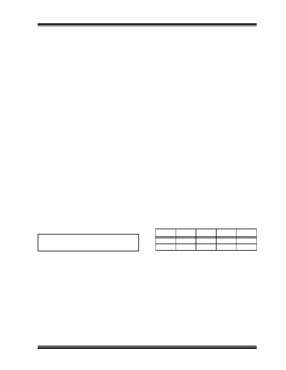
TABLE 5-1:
TC1303A, TC1303B, TC1303C,
TC1304 RECOMMENDED
CAPACITOR VALUES
RTOP = 200 k
VOUT1 =2.1V
VFB =0.8V
RBOT = 200 k x (0.8V/(2.1V – 0.8V))
RBOT = 123 k (Standard Value = 121 k)
RCOMP =4.99 k
CCOMP =33 pF
R
BOT
R
TOP
V
FB
V
OUT1
V
FB
–
--------------------------------
×
=
C(VIN1)C(VIN2)COUT1
COUT2
min
4.7 F
none
4.7 F
1 F
max
none
22 F
10 F
相关PDF资料 |
PDF描述 |
|---|---|
| TC1303A-1L0EMF | 0.5 A SWITCHING REGULATOR, 2400 kHz SWITCHING FREQ-MAX, PDSO10 |
| TC1303A-1S0EUNTR | 0.5 A SWITCHING REGULATOR, 2400 kHz SWITCHING FREQ-MAX, PDSO10 |
| TC1303A-AF1EMFTR | 0.5 A SWITCHING REGULATOR, 2400 kHz SWITCHING FREQ-MAX, PDSO10 |
| TC1303A-AF2EUNTR | 0.5 A SWITCHING REGULATOR, 2400 kHz SWITCHING FREQ-MAX, PDSO10 |
| TC1303A-AK0EMF | 0.5 A SWITCHING REGULATOR, 2400 kHz SWITCHING FREQ-MAX, PDSO10 |
相关代理商/技术参数 |
参数描述 |
|---|---|
| TC1305R-DVUN | 功能描述:低压差稳压器 - LDO Dual LDO w/ Sdn RoHS:否 制造商:Texas Instruments 最大输入电压:36 V 输出电压:1.4 V to 20.5 V 回动电压(最大值):307 mV 输出电流:1 A 负载调节:0.3 % 输出端数量: 输出类型:Fixed 最大工作温度:+ 125 C 安装风格:SMD/SMT 封装 / 箱体:VQFN-20 |
| TC1305R-DVUNTR | 功能描述:低压差稳压器 - LDO Dual LDO w/ Sdn RoHS:否 制造商:Texas Instruments 最大输入电压:36 V 输出电压:1.4 V to 20.5 V 回动电压(最大值):307 mV 输出电流:1 A 负载调节:0.3 % 输出端数量: 输出类型:Fixed 最大工作温度:+ 125 C 安装风格:SMD/SMT 封装 / 箱体:VQFN-20 |
| TC1306R-BDVUA | 功能描述:低压差稳压器 - LDO Dual LDO w/ Sdn RoHS:否 制造商:Texas Instruments 最大输入电压:36 V 输出电压:1.4 V to 20.5 V 回动电压(最大值):307 mV 输出电流:1 A 负载调节:0.3 % 输出端数量: 输出类型:Fixed 最大工作温度:+ 125 C 安装风格:SMD/SMT 封装 / 箱体:VQFN-20 |
| TC1306R-BDVUATR | 功能描述:低压差稳压器 - LDO Dual LDO w/ Sdn RoHS:否 制造商:Texas Instruments 最大输入电压:36 V 输出电压:1.4 V to 20.5 V 回动电压(最大值):307 mV 输出电流:1 A 负载调节:0.3 % 输出端数量: 输出类型:Fixed 最大工作温度:+ 125 C 安装风格:SMD/SMT 封装 / 箱体:VQFN-20 |
| TC1307R-XYVQRTR | 功能描述:低压差稳压器 - LDO Dual LDO w/ Sdn RoHS:否 制造商:Texas Instruments 最大输入电压:36 V 输出电压:1.4 V to 20.5 V 回动电压(最大值):307 mV 输出电流:1 A 负载调节:0.3 % 输出端数量: 输出类型:Fixed 最大工作温度:+ 125 C 安装风格:SMD/SMT 封装 / 箱体:VQFN-20 |
发布紧急采购,3分钟左右您将得到回复。