- 您现在的位置:买卖IC网 > PDF目录383915 > TC1305R-DVUN (Microchip Technology Inc.) Circular Connector; MIL SPEC:MIL-C-26482, Series I, Solder; Body Material:Aluminum; Series:PT06; Number of Contacts:10; Connector Shell Size:12; Connecting Termination:Solder; Circular Shell Style:Straight Plug; Body Style:Straight PDF资料下载
参数资料
| 型号: | TC1305R-DVUN |
| 厂商: | Microchip Technology Inc. |
| 元件分类: | 圆形连接器 |
| 英文描述: | Circular Connector; MIL SPEC:MIL-C-26482, Series I, Solder; Body Material:Aluminum; Series:PT06; Number of Contacts:10; Connector Shell Size:12; Connecting Termination:Solder; Circular Shell Style:Straight Plug; Body Style:Straight |
| 中文描述: | 双150mA的CMOS低压与选择模式⑩行动,关闭和独立RESET输出 |
| 文件页数: | 2/18页 |
| 文件大小: | 530K |
| 代理商: | TC1305R-DVUN |
TC1305
DS21526A-page 2
2002 Microchip Technology Inc.
1.0
ELECTRICAL
CHARACTERISTICS
ABSOLUTE MAXIMUM RATINGS*
Input Voltage .........................................................6.5V
Output Voltage...........................(-0.3V) to (V
IN
+ 0.3V)
Power Dissipation................Internally Limited
(Note 7)
Maximum Voltage on Any Pin .........V
IN
+0.3V to -0.3V
Operating Temperature Range....-40°C < T
J
< +125°C
Storage Temperature Range..............-55°C to +150°C
*Stresses above those listed under "Absolute Maximum
Ratings" may cause permanent damage to the device. These
are stress ratings only and functional operation of the device
at these or any other conditions above those indicated in the
operation sections of the specifications is not implied.
Exposure to Absolute Maximum Rating conditions for
extended periods may affect device reliability.
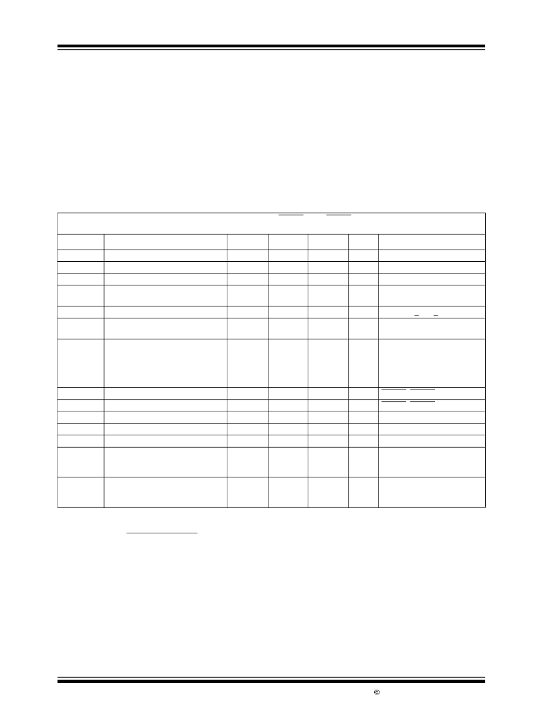
TC1305 ELECTRICAL SPECIFICATIONS
Electrical Characteristics:
V
IN
= V
R
+ 1V, I
L
= 100
μ
A, C
L
= 3.3
μ
F, SHDN1 > V
IH
, SHDN2 > V
IH
, T
A
= 25°C, unless otherwise
noted.
Boldface
type specifications apply for junction temperature of -40°C to +125°C. Applies to both V
OUT1
and V
OUT2
.
Symbol
Parameter
Min
Typ
Max
Units
Test Conditions
V
IN
I
OUT
MAX
V
OUT
TCV
OUT
Input Operating Voltage
Maximum Output Current
Output Voltage (V
OUT1
and V
OUT2
)
V
OUT
Temperature Coefficient
2.7
150
—
—
6.0
—
V
Note 1
Per Channel
Note 2
mA
V
V
R
– 2.5%
V
R
± 0.5%
V
R
+ 2.5%
—
—
40
—
0.05
—
0.5
20
—
—
0.35
2
ppm/°C
Note 3
V
OUT
/
V
IN
V
OUT
/V
OUT
Load Regulation
Line Regulation
%
%
(V
R
+ 1V) < V
IN
< 6V
I
L
= 0.1mA to I
OUT
MAX
(Note 4)
I
L
= 100
μ
A
I
L
= 50mA
I
L
= 100mA
I
L
= 150mA
(Note 5)
SHDN1, SHDN2 = V
IH
, I
L
= 0
SHDN1, SHDN2 = 0V
F
RE
≤
120Hz
V
OUT
= 0V
Notes 6, 7
V
IN
= 5V
C
IN
= 1
μ
F, C
OUT
= 4.7
μ
F
I
L
= 30mA, (See Figure 4-1)
V
IN
= 5V
C
IN
= 1
μ
F, C
OUT
= 4.7
μ
F
I
L
= 30mA, (See Figure 4-1)
V
IN –
V
OUT
Dropout Voltage
—
2
50
100
150
—
120
240
360
mV
I
IN
I
INSD
PSRR
I
OUTSC
V
OUT
P
D
t
WK
Supply Current
Shutdown Supply Current
Power Supply Rejection Ratio
Output Short Circuit Current
Thermal Regulation
Wake Up Time
—
—
—
—
—
—
120
0.05
64
600
0.04
10
160
0.5
—
—
—
—
μ
A
μ
A
dB
mA
V/W
μ
sec
(from Shutdown Mode)
Settling Time
ts
(from Shutdown Mode)
—
40
—
μ
sec
Note 1:
The minimum V
has to meet two conditions: V
≥
2.7 and V
≥
V
+ V
.
V
R
is the regulator output voltage setting. For example: V
R
= 2.5V, 2.8V, 3.0V.
T
C
V
OUT
= (V
OUT
MAX
– V
OUT
MIN
) x 10
6
V
OUT
x
T
2:
3:
4:
Regulation is measured at a constant junction temperature using low duty cycle pulse testing. Load regulation is tested over a load range from
0.1mA to the maximum specified output current. Changes in output voltage due to heating effects are covered by the thermal regulation
specification.
Dropout voltage is defined as the input to output differential at which the output voltage drops2% below its nominal value measured at a 1V
differential.
Thermal Regulation is defined as the change in output voltage at a time T after a change in power dissipation is applied, excluding load or
line regulation effects. Specifications are for a current pulse equal to I
at V
= 6V for T = 10 msec.
The maximum allowable power dissipation is a function of ambient temperature, the maximum allowable junction temperature and the
thermal resistance from junction-to-air (i.e., T
, T
,
θ
). Exceeding the maximum allowable power dissipation causes the device to initiate
thermal shutdown. Please see Section 5.0 Thermal Considerations section of this data sheet for more details.
5:
6:
7:
相关PDF资料 |
PDF描述 |
|---|---|
| TC1306 | Dual 150mA CMOS LDOWith Select Mode⑩ Operation, Shutdown and RESET Output |
| TC1306R-BDVUA | Circular Connector; Body Material:Aluminum; Series:PT07; No. of Contacts:19; Connector Shell Size:14; Connecting Termination:Solder; Circular Shell Style:Jam Nut Receptacle; Circular Contact Gender:Socket; Insert Arrangement:14-19 |
| TC1307 | Four-Channel CMOS LDO with Select Mode, Shutdown and Independent Reset |
| TC1313-CL0EMFTR | 500 mA Synchronous Buck Regulator, + 300 mA LDO |
| TC1313-CL0EUN | 500 mA Synchronous Buck Regulator, + 300 mA LDO |
相关代理商/技术参数 |
参数描述 |
|---|---|
| TC1305R-DVUNTR | 功能描述:低压差稳压器 - LDO Dual LDO w/ Sdn RoHS:否 制造商:Texas Instruments 最大输入电压:36 V 输出电压:1.4 V to 20.5 V 回动电压(最大值):307 mV 输出电流:1 A 负载调节:0.3 % 输出端数量: 输出类型:Fixed 最大工作温度:+ 125 C 安装风格:SMD/SMT 封装 / 箱体:VQFN-20 |
| TC1306R-BDVUA | 功能描述:低压差稳压器 - LDO Dual LDO w/ Sdn RoHS:否 制造商:Texas Instruments 最大输入电压:36 V 输出电压:1.4 V to 20.5 V 回动电压(最大值):307 mV 输出电流:1 A 负载调节:0.3 % 输出端数量: 输出类型:Fixed 最大工作温度:+ 125 C 安装风格:SMD/SMT 封装 / 箱体:VQFN-20 |
| TC1306R-BDVUATR | 功能描述:低压差稳压器 - LDO Dual LDO w/ Sdn RoHS:否 制造商:Texas Instruments 最大输入电压:36 V 输出电压:1.4 V to 20.5 V 回动电压(最大值):307 mV 输出电流:1 A 负载调节:0.3 % 输出端数量: 输出类型:Fixed 最大工作温度:+ 125 C 安装风格:SMD/SMT 封装 / 箱体:VQFN-20 |
| TC1307R-XYVQRTR | 功能描述:低压差稳压器 - LDO Dual LDO w/ Sdn RoHS:否 制造商:Texas Instruments 最大输入电压:36 V 输出电压:1.4 V to 20.5 V 回动电压(最大值):307 mV 输出电流:1 A 负载调节:0.3 % 输出端数量: 输出类型:Fixed 最大工作温度:+ 125 C 安装风格:SMD/SMT 封装 / 箱体:VQFN-20 |
| TC130AW10 | 制造商:Panduit Corp 功能描述: |
发布紧急采购,3分钟左右您将得到回复。