- 您现在的位置:买卖IC网 > PDF目录98168 > TC1321IUATR 10-BIT DAC, PDSO8 PDF资料下载
参数资料
| 型号: | TC1321IUATR |
| 元件分类: | DAC |
| 英文描述: | 10-BIT DAC, PDSO8 |
| 封装: | PLASTIC, MSOP-8 |
| 文件页数: | 18/24页 |
| 文件大小: | 523K |
| 代理商: | TC1321IUATR |
2010 Microchip Technology Inc.
DS21387C-page 3
TC1321
1.0
ELECTRICAL
CHARACTERISTICS
Absolute Maximum Ratings*
Supply Voltage (VDD) ........................................................+6V
Voltage on any Pin ....................(VSS – 0.3V) to (VDD + 0.3V)
Current on any Pin ......................................................±50 mA
Package Thermal Resistance (
JA)....................... 330°C C/W
Operating Temperature (TA)...................................See Below
Storage Temperature (TSTG).........................-65°C to +150°C
*Stresses above those listed under “Absolute Maximum
Ratings” may cause permanent damage to the device. These
are stress ratings only and functional operation of the device
at these or any other conditions above those indicated in the
operation sections of the specifications is not implied.
Exposure to Absolute Maximum Rating conditions for
extended periods may affect device reliability.
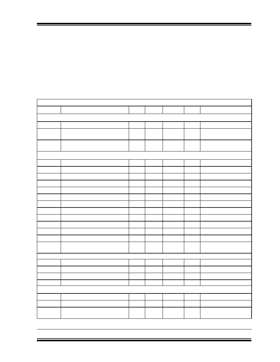
ELECTRICAL SPECIFICATIONS
Electrical Characteristics: VDD = 2.7V to 5.5V, -40°C TA +85°C, VREF = 1.2 V unless otherwise noted.
Symbol
Parameter
Min
Typ
Max
Unit
Test Conditions
Power Supply
VDD
Supply Voltage
2.7
—
5.5
V
IDD
Operating Current
—
350
500
A
VDD = 5.5V, VREF = 1.2V
Serial Port Inactive (Note 1)
IDD-
STANDBY
Standby Supply Current
—
0.1
1
A
VDD = 3.3V
Serial Port Inactive (Note 1)
Static Performance - Analog Section
Resolution
—
10
Bits
INL
Integral Non-Linearity at FS, TA = +25°C
—
±4.0
LSB
FSE
Full Scale Error
—
±3
%FS
DNL
Differential Non-Linearity, TA = +25°C
-1
—
+2
LSB
All Codes (Note 2)
VOS
Offset Error at VOUT
—±0.3
±8
mV
TCVOS
Offset Error Tempco at VOUT
—10
—
v/°C
PSRR
Power Supply Rejection Ratio
—
80
—
dB
VDD at DC
VREF
Voltage Reference Range
0
—
VDD – 1.2
V
IREF
Reference Input Leakage Current
—
±1.0
A
VSW
Voltage Swing
0
—
VREF
VVREF (VDD – 1.2V)
ROUT
Output Resistance @ VOUT
—5.0
—
ROUT ()
IOUT
Output Current (Source or Sink)
—
2
—
mA
ISC
Output Short-Circuit Current
VDD = 5.5V
—
30
20
50
mA
Source
Sink
Dynamic Performance
SR
Voltage Output Slew Rate
—
0.8
—
V/s
tSETTLE
Output Voltage Full Scale Settling Time
—
10
—
s
tWU
Wake-up Time
—
20
—
s
Digital Feed Through and Crosstalk
—
5
—
nV-s
SDA = VDD, SCL = 100 kHz
Serial Port Interface
VIH
Logic Input High
2.4
—
VDD
V
VIL
Logic Input Low
—
0.6
—
VOL
SDA Output Low
—
0.4
0.6
V
IOL = 3 mA (Sinking Current)
IOL = 6 mA
Note 1: SDA and SCL must be connected to VDD or VSS.
2: Measured at VOUT 50 mV referred to VSS to avoid output buffer clipping.
相关PDF资料 |
PDF描述 |
|---|---|
| TC1321IOA | 10-BIT DAC, PDSO8 |
| TC1321IOATR | 10-BIT DAC, PDSO8 |
| TC1321IUA | 10-BIT DAC, PDSO8 |
| TC1322EOART | SERIAL INPUT LOADING, 10 us SETTLING TIME, 12-BIT DAC, PDSO8 |
| TC1322EUART | SERIAL INPUT LOADING, 10 us SETTLING TIME, 12-BIT DAC, PDSO8 |
相关代理商/技术参数 |
参数描述 |
|---|---|
| TC-133.330MBD-T | 功能描述:标准时钟振荡器 133.330MHz 3.3V 25ppm -40C to 85C RoHS:否 制造商:AVX 产品:Standard Clock Oscillators 封装 / 箱体:7 mm x 5 mm 频率:75 MHz 频率稳定性:50 PPM 电源电压:2.5 V 负载电容: 端接类型:SMD/SMT 最小工作温度:0 C 最大工作温度:+ 70 C 输出格式:LVDS 尺寸: 封装:Reel 系列: |
| TC-133.330MBE-T | 制造商:TXC Corporation 功能描述:OSC MEMS 133.330 MHZ 3.3V SMD |
| TC-133.330MCD-T | 功能描述:标准时钟振荡器 133.330MHz 2.5V 25ppm -40C to 85C RoHS:否 制造商:AVX 产品:Standard Clock Oscillators 封装 / 箱体:7 mm x 5 mm 频率:75 MHz 频率稳定性:50 PPM 电源电压:2.5 V 负载电容: 端接类型:SMD/SMT 最小工作温度:0 C 最大工作温度:+ 70 C 输出格式:LVDS 尺寸: 封装:Reel 系列: |
| TC-133.330MCE-T | 制造商:TXC Corporation 功能描述:OSC MEMS 133.330 MHZ 2.5V SMD |
| TC-13C | 制造商:Panduit Corp 功能描述: |
发布紧急采购,3分钟左右您将得到回复。