- 您现在的位置:买卖IC网 > PDF目录85452 > TC1684EUATR SWITCHED CAPACITOR CONVERTER, 170 kHz SWITCHING FREQ-MAX, PDSO8 PDF资料下载
参数资料
| 型号: | TC1684EUATR |
| 元件分类: | 稳压器 |
| 英文描述: | SWITCHED CAPACITOR CONVERTER, 170 kHz SWITCHING FREQ-MAX, PDSO8 |
| 封装: | MSOP-8 |
| 文件页数: | 6/10页 |
| 文件大小: | 228K |
| 代理商: | TC1684EUATR |
2005 Microchip Technology Inc.
DS21537C-page 5
TC1682/TC1683/TC1684
4.0
APPLICATIONS INFORMATION
4.1
Output Voltage Considerations
The
TC1682/TC1683/TC1684
perform
inverting
voltage conversions but do not provide any type of
regulation. The output voltage will droop in a linear
manner with respect to the output load current. The
value
of
the
equivalent
output
resistance
is
approximately 120
Ω nominal at +25°C and VIN = +5V.
In this particular case, the output is approximately -10V
at very light loads and will droop according to the
equation below:
VDROOP = IOUT x ROUT
4.2
Capacitor Selection
In order to maintain the lowest output resistance and
output ripple voltage, it is recommended that low ESR
capacitors be used. Additionally, larger values of C1
and C2 will lower the output resistance and larger
values of COUT will reduce output ripple.
Note:
For proper charge pump operation, C1
must have a voltage rating greater than or
equal to VIN, while C2 and COUT must have
a voltage rating greater than or equal to
2VIN.
Table 4-1 shows various values of C1/C2 and the
corresponding output resistance values for VIN = 5V
@ +25°C.
Table 4-2 shows the output voltage ripple for various
values of COUT (again assuming VIN = 5V @ +25°C).
The VRIPPLE values assume a 1mA output load current
and a 0.1
Ω ESRCOUT.
TABLE 4-1:
OUTPUT RESISTANCE
VS. C1/C2 (ESR = 0.1
Ω)
TABLE 4-2:
OUTPUT VOLTAGE RIPPLE
VS. COUT2 (ESR = 0.1Ω)
IOUT = 1mA
4.3
Input Supply Bypassing
The VIN input should be capacitively bypassed to
reduce AC impedance and minimize noise effects due
to
the
switching
internal
to
the
device.
It
is
recommended that a large value capacitor (at least
equal to C1) be connected from VIN to GND for optimal
circuit performance.
4.4
Shutdown Input
The TC1682/TC1683/TC1684 is enabled when SHDN
is low, and disabled when SHDN is high. This input
cannot be allowed to float. (If SHDN is not required, see
the TC2682/TC2683/TC2684 data sheet.) The SHDN
input should be limited to 0.3V above VIN.
4.5
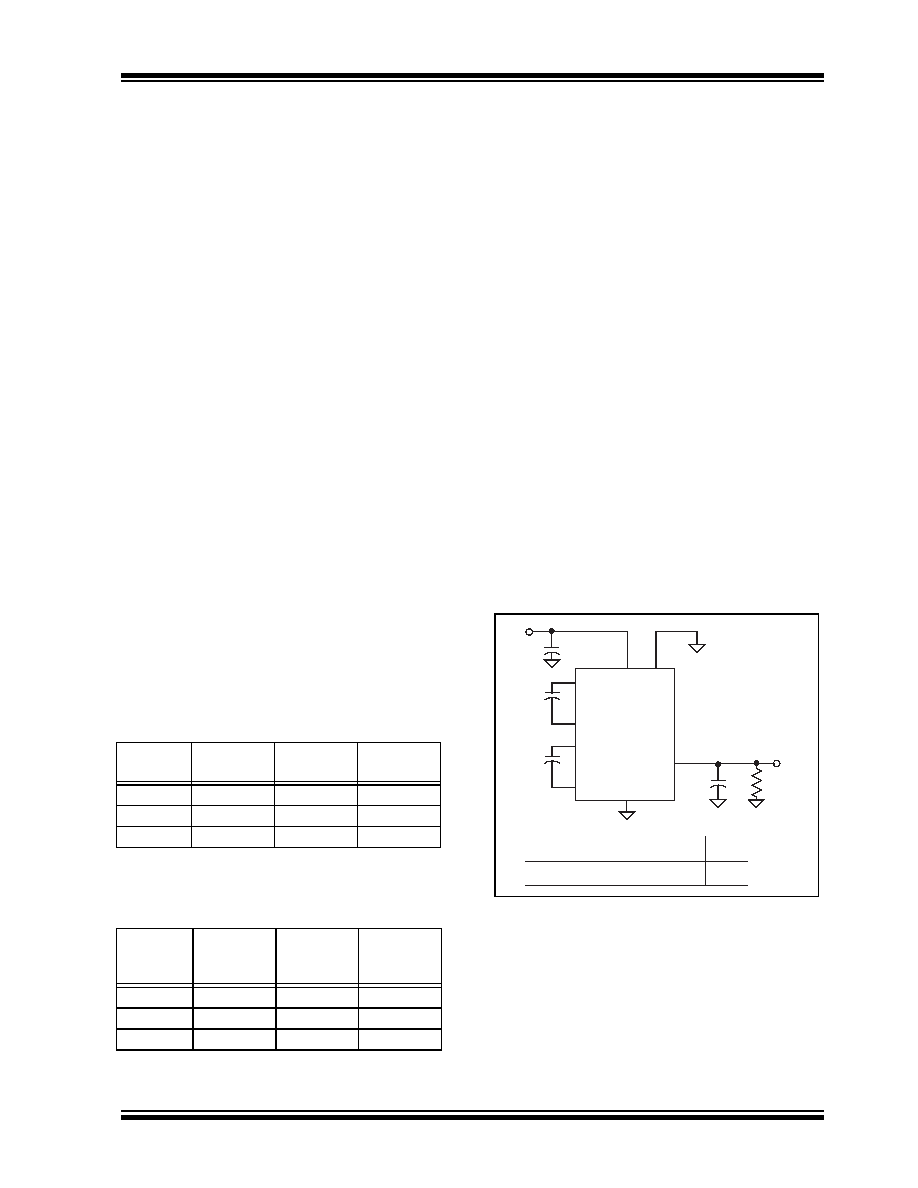
Inverting Voltage Doubler
The most common application for the TC1682/TC1683/
TC1684 devices is the inverting voltage doubler
(Figure 4-1). This application uses three external
capacitors: C1, C2 and COUT.
Note:
A
power
supply
bypass
capacitor
is
recommended.
The output is equal to -2VIN plus any voltage drops due
capacitor selection guidelines.
FIGURE 4-1:
INVERTING VOLTAGE
DOUBLER TEST CIRCUIT
4.6
Layout Considerations
As with any switching power supply circuit, good layout
practice is recommended. Mount components as close
together as possible to minimize stray inductance and
capacitance. Also use a large ground plane to minimize
noise leakage into other circuitry.
C1, C2
(
μF)
TC1682
ROUT(Ω)
TC1683
ROUT(Ω)
TC1684
ROUT(Ω)
0.33
633
184
120
1
262
120
102
3.3
120
95
84
COUT
(
μF)
TC1682
VRIPPLE
(mV)
TC1683
VRIPPLE
(mV)
TC1684
VRIPPLE
(mV)
0.33
192
60
27
163
21
16
3.3
17
8
7
C1
C2
VIN
CIN
VOUT
RL
VIN
COUT
TC1682
TC1683
TC1684
C1–
C2–
2
1
7
6
8
4
5
3
C1+
C2+
GND
+
Device
CIN
C1
C2
COUT
TC1682
3.3
μF
3.3
μF
3.3
μF
3.3
μF
TC1683
1
μF
1
μF
1
μF
1
μF
TC1684
0.33
μF
0.33
μF
0.33
μF
0.33
μF
SHDN
VOUT
相关PDF资料 |
PDF描述 |
|---|---|
| TC52N1524ECTTR | 2-CHANNEL POWER SUPPLY SUPPORT CKT, PDSO5 |
| TC52N1637ECTTR | 2-CHANNEL POWER SUPPLY SUPPORT CKT, PDSO5 |
| TC52N2427ECTTR | 2-CHANNEL POWER SUPPLY SUPPORT CKT, PDSO5 |
| TC52N2434ECTTR | 2-CHANNEL POWER SUPPLY SUPPORT CKT, PDSO5 |
| TC52N2550ECTTR | 2-CHANNEL POWER SUPPLY SUPPORT CKT, PDSO5 |
相关代理商/技术参数 |
参数描述 |
|---|---|
| TC1-6-ST 305SS | 制造商:RIVETS 功能描述: |
| TC1-6-ST NKL BR | 制造商:RIVETS 功能描述: |
| TC16V | 制造商:TAK_CHEONG 制造商全称:Tak Cheong Electronics (Holdings) Co.,Ltd 功能描述:500 mW DO-35 Hermetically Sealed Glass Zener Voltage Regulators |
| TC-16Y | 功能描述:打印机 LS6, Component Label, Polyester, 2.00"(5 RoHS:否 制造商:Seiko Instruments 产品:Printer 电源电压: 每行点数:9 x 320 打印速度:52.5 cps, 80 cps 纸张宽度:112 mm |
| TC170 | 制造商:MICROCHIP 制造商全称:Microchip Technology 功能描述:CMOS Current Mode PWM Controller |
发布紧急采购,3分钟左右您将得到回复。