- 您现在的位置:买卖IC网 > PDF目录98169 > TC3400VPA 1-CH 16-BIT DELTA-SIGMA ADC, SERIAL ACCESS, PDIP8 PDF资料下载
参数资料
| 型号: | TC3400VPA |
| 元件分类: | ADC |
| 英文描述: | 1-CH 16-BIT DELTA-SIGMA ADC, SERIAL ACCESS, PDIP8 |
| 封装: | PLASTIC, DIP-8 |
| 文件页数: | 13/16页 |
| 文件大小: | 437K |
| 代理商: | TC3400VPA |
TC3400
DS21409B-page 6
2002 Microchip Technology Inc.
3.0
DETAILED DESCRIPTION
The TC3400 is a 16-bit sigma-delta A/D converter with
one differential input. See the Typical Application circuit
and the Functional Block diagram. The key components
of the TC3400 are described below.
Also refer to Figure 3-4, A/D Operational Flowchart and
the Timing Diagrams, Figure 3-1, Figure 3-2 and
Figure 3-3).
3.1
A/D Converter Operation
When the TC3400 is not converting, it is in sleep mode
with both the SCLK and SDAT lines high. An A/D
conversion is initiated by a high to low transition on the
SCLK line at which time the internal clock of the
TC3400 is started. Each additional high to low
transition of SCLK (following the initial SCLK falling
edge) during the time interval t4, will decrement the
conversion resolution by one bit and reduce the
conversion time by one half. The time interval t4 is
referred to as the resolution reduction window. The
minimum conversion resolution is 10-bits so any more
than 6 SCLK transitions during t4 will be ignored.
After each high to low transition of SCLK, in the t4
interval, the SDAT output is driven high by the TC3400
to acknowledge that the conversion has been decre-
mented. When the SCLK returns high or the t4 interval
ends, the SDAT line returns low (see Figure 3-2). When
the conversion is complete SDAT is driven high. The
TC3400 now enters sleep mode and the conversion
value can be read as a serial data word on the SDAT
line.
3.2
Reading the Data Word
After the conversion is complete and SDAT goes high,
the conversion value can be clocked serially onto the
SDAT line by high to low transitions of the SCLK. The
data word is in two’s compliment format with the sign bit
clocked onto the SDAT line, first followed by the MSB
and ending in the LSB. For a 16-bit conversion the data
word would consist of a sign bit followed by 15 magni-
tude bits, Table 3-1 shows the data word versus input
voltage for a 16-bit conversion. Note that the full scale
input voltage range is ±(2 REFIN – 1LSB). When
REFOUT is fed back directly to REFIN,an LSB is 73V
for a 16-bit conversion, as REFOUT is typically 1.193V.
Figure 3-3 shows typical SCLK and SDAT waveforms
for 16, 12 and 10-bit conversions. Note that any
complete convert and read cycle requires 17 negative
edge clock pulses. The first is the convert command.
Then, up to six of these can occur in the resolution
reduction window, t4, to decrement resolution. The
remaining pulses clock out the conversion data word.
TABLE 3-1:
DATA CONVERSION WORD
VS. VOLTAGE INPUT
(REFIN = 1.193V)
The SCLK input has a filter which rejects any positive
or negative pulse of width less than 50nsec to reduce
noise. The rejection width of this pulse can vary
between 50nsec and 750nsec depending on process-
ing parameters and supply voltage.
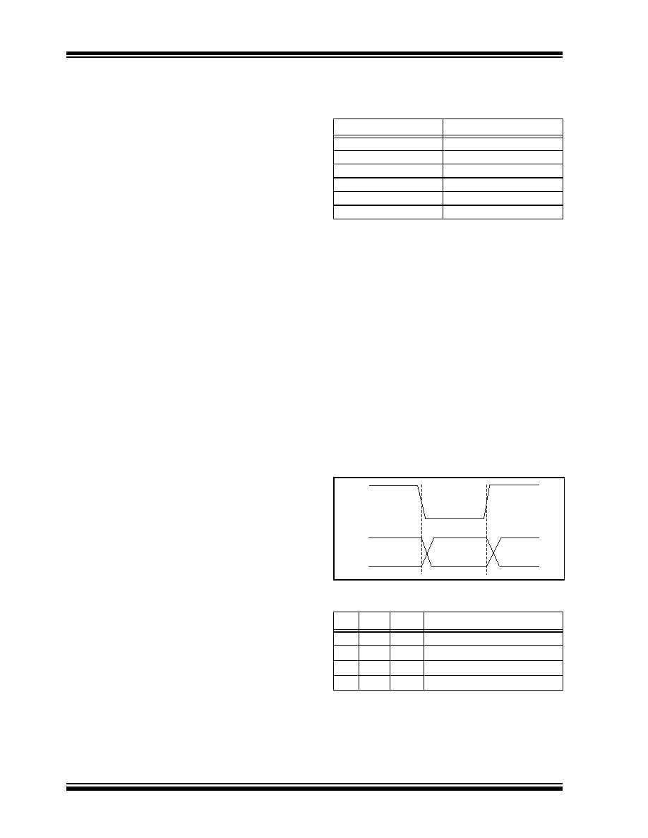
Figure 3-1 and Table 3-2 show information for deter-
mining the mode of operation for the TC3400 part by
recording the value of SDAT for SCLK in a high, then
low, then high state. For example, if SCLK goes
through a 1-0-1 transition and the corresponding val-
ues of SDAT are 1-1-0, then the SCLK falling edge
started a new data conversion. A 0-1-0 for SDAT would
have indicated a resolution reduction had occurred.
This is useful if the microcontroller has a watchdog
reset or otherwise loses track of where the TC3400 is
in the conversion and data readout sequence. The
microcontroller can simply transition SCLK until it
“finds” a Start Conversion condition.
FIGURE 3-1:
SCLK, SDAT LOGIC
STATE DIAGRAM
TABLE 3-2:
SCLK, SDAT LOGIC STATE
*Note: The code X00 has a dual meaning: Data Transfer or
Busy converting. To avoid confusion, the user should
send only the required number of pulses for the
desired resolution, then wait for SDAT to rise to 1,
indicating conversion is complete before clocking
SCLK again to read out data bits.
Data Word
INn+ –INn- (Volts)
0111 1111 1111 1111
2.38596 (Positive Full Scale)
0000 0000 0000 0001
72.8 E -6
0000 0000 0000 0000
0
1111 1111 1111 1111
-72.8 E -6
1000 0000 0000 0001
-2.38596 (Negative Full Scale)
1000 0000 0000 0000
Reserved Code
AB
C
Status
1
0
Start Conversion
0
1
0
Resolution Reduction
x
1
Data Transfer
x
0
Data Transfer or Busy*
SCLK
SDAT
A
BC
相关PDF资料 |
PDF描述 |
|---|---|
| TC3401EQR | 2-CH 16-BIT DELTA-SIGMA ADC, SERIAL ACCESS, PDSO16 |
| TC3401EPE | 2-CH 16-BIT DELTA-SIGMA ADC, SERIAL ACCESS, PDIP16 |
| TC3401EPE | 2-CH 16-BIT DELTA-SIGMA ADC, SERIAL ACCESS, PDIP16 |
| TC3401EQR | 2-CH 16-BIT DELTA-SIGMA ADC, SERIAL ACCESS, PDSO16 |
| TC3401VPE | 2-CH 16-BIT DELTA-SIGMA ADC, SERIAL ACCESS, PDIP16 |
相关代理商/技术参数 |
参数描述 |
|---|---|
| TC3401 | 制造商:MICROCHIP 制造商全称:Microchip Technology 功能描述:16-Bit Low Cost, Low Power Sigma-Delta A/D Converter |
| TC3401VPE | 功能描述:模数转换器 - ADC 16-Bit Sigma-Delta RoHS:否 制造商:Texas Instruments 通道数量:2 结构:Sigma-Delta 转换速率:125 SPs to 8 KSPs 分辨率:24 bit 输入类型:Differential 信噪比:107 dB 接口类型:SPI 工作电源电压:1.7 V to 3.6 V, 2.7 V to 5.25 V 最大工作温度:+ 85 C 安装风格:SMD/SMT 封装 / 箱体:VQFN-32 |
| TC3401VQR | 功能描述:模数转换器 - ADC 16-Bit Sigma-Delta RoHS:否 制造商:Texas Instruments 通道数量:2 结构:Sigma-Delta 转换速率:125 SPs to 8 KSPs 分辨率:24 bit 输入类型:Differential 信噪比:107 dB 接口类型:SPI 工作电源电压:1.7 V to 3.6 V, 2.7 V to 5.25 V 最大工作温度:+ 85 C 安装风格:SMD/SMT 封装 / 箱体:VQFN-32 |
| TC3401VQRTR | 功能描述:模数转换器 - ADC 16-Bit Sigma-Delta RoHS:否 制造商:Texas Instruments 通道数量:2 结构:Sigma-Delta 转换速率:125 SPs to 8 KSPs 分辨率:24 bit 输入类型:Differential 信噪比:107 dB 接口类型:SPI 工作电源电压:1.7 V to 3.6 V, 2.7 V to 5.25 V 最大工作温度:+ 85 C 安装风格:SMD/SMT 封装 / 箱体:VQFN-32 |
| TC3402 | 制造商:MICROCHIP 制造商全称:Microchip Technology 功能描述:+1.8 Low Power, Quad Input, 16-Bit Sigma-Delta A/D Converter |
发布紧急采购,3分钟左右您将得到回复。