- 您现在的位置:买卖IC网 > Datasheet目录365 > TC4424MJA (Microchip Technology)IC MOSFET DVR 3A DUAL HS 8-CDIP Datasheet资料下载
参数资料
| 型号: | TC4424MJA |
| 厂商: | Microchip Technology |
| 文件页数: | 9/18页 |
| 文件大小: | 0K |
| 描述: | IC MOSFET DVR 3A DUAL HS 8-CDIP |
| 标准包装: | 56 |
| 配置: | 低端 |
| 输入类型: | 非反相 |
| 延迟时间: | 33ns |
| 电流 - 峰: | 3A |
| 配置数: | 2 |
| 输出数: | 2 |
| 电源电压: | 4.5 V ~ 18 V |
| 工作温度: | -55°C ~ 125°C |
| 安装类型: | 通孔 |
| 封装/外壳: | 8-CDIP(0.300",7.62mm) |
| 供应商设备封装: | 8-CERDIP |
| 包装: | 管件 |
�� �
�
�TC4423M/TC4424M/TC4425M�
�3.0�
�PIN� DESCRIPTIONS�
�3.4�
�Output� A� (OUT� A)�
�The� descriptions� of� the� pins� are� listed� in� Table� 3-1.�
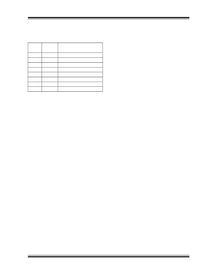
�TABLE� 3-1:� PIN� FUNCTION� TABLE�
�8-Pin�
�Symbol� Description�
�CERDIP�
�OUT� A� is� a� CMOS,� push-pull� output� that� is� capable� of�
�sourcing� and� sinking� 3A� peaks� of� current� (V� DD� =� 18V).�
�The� low� output� impedance� ensures� the� gate� of� the�
�external� MOSFET� will� stay� in� the� intended� state� even�
�during� large� transients.� This� output� also� has� a� reverse�
�current� latch-up� rating� of� 1.5A.�
�1�
�2�
�NC�
�IN� A�
�No� connection�
�Input� A�
�3.5�
�Supply� Input� (V� DD� )�
�3�
�4�
�5�
�6�
�7�
�GND�
�IN� B�
�OUT� B�
�V� DD�
�OUT� A�
�Ground�
�Input� B�
�Output� B�
�Supply� input�
�Output� A�
�V� DD� is� the� bias� supply� input� for� the� MOSFET� driver� and�
�has� a� voltage� range� of� 4.5V� to� 18V.� This� input� must� be�
�decoupled� to� ground� with� a� local� ceramic� capacitor.�
�This� bypass� capacitor� provides� a� localized� low-�
�impedance� path� for� the� peak� currents� that� are� to� be�
�provided� to� the� load.�
�8�
�NC�
�No� connection�
�3.6�
�Ground� (GND)�
�GND� is� the� device� return� pin.� The� ground� pin(s)� should�
�3.1�
�Input� A� (IN� A)�
�have� a� low-impedance� connection� to� the� bias� supply�
�source� return.� High� peak� currents� will� flow� out� the�
�IN� A� is� a� TTL/CMOS-compatible� input� that� controls�
�OUT� A.� This� input� has� 300� mV� of� hysteresis� between�
�the� high� and� low� input� levels� that� allows� it� to� be� driven�
�from� slow� rising� and� falling� signals,� as� well� as� providing�
�noise� immunity.�
�ground� pin(s)� when� the� capacitive� load� is� being�
�discharged.�
�3.2�
�Input� B� (IN� B)�
�IN� B� is� a� TTL/CMOS-compatible� input� that� controls�
�OUT� B.� This� input� has� 300� mV� of� hysteresis� between�
�the� high� and� low� input� levels� that� allows� it� to� be� driven�
�from� slow� rising� and� falling� signals,� as� well� as� providing�
�noise� immunity.�
�3.3�
�Output� B� (OUT� B)�
�OUT� B� is� a� CMOS� push-pull� output� that� is� capable� of�
�sourcing� and� sinking� 3A� peaks� of� current� (V� DD� =� 18V).�
�The� low� output� impedance� ensures� the� gate� of� the�
�external� MOSFET� will� stay� in� the� intended� state� even�
�during� large� transients.� This� output� also� has� a� reverse�
�current� latch-up� rating� of� 1.5A.�
�?� 2005� Microchip� Technology� Inc.�
�DS21937A-page� 9�
�相关PDF资料 |
PDF描述 |
|---|---|
| TC4425VMF | IC MOSFET DVR 3A DUAL HS 8DFN |
| TC4427MJA | IC MOSFET DVR 1.5A DUAL HS 8CDIP |
| TC4428VUA713 | IC MOSFET DVR 1.5A DUAL HS 8MSOP |
| TC4429VPA | IC MOSFET DRIVER 6A HS 8DIP |
| TC4432VOA713 | IC MOSFET DRIVER 30V 1.5A 8SOIC |
相关代理商/技术参数 |
参数描述 |
|---|---|
| TC4424VG | 制造商:MICROCHIP 制造商全称:Microchip Technology 功能描述:3A Dual High-Speed Power MOSFET Drivers |
| TC4424VMF | 功能描述:功率驱动器IC 3A Dual RoHS:否 制造商:Micrel 产品:MOSFET Gate Drivers 类型:Low Cost High or Low Side MOSFET Driver 上升时间: 下降时间: 电源电压-最大:30 V 电源电压-最小:2.75 V 电源电流: 最大功率耗散: 最大工作温度:+ 85 C 安装风格:SMD/SMT 封装 / 箱体:SOIC-8 封装:Tube |
| TC4424VMF713 | 功能描述:功率驱动器IC 3A Dual RoHS:否 制造商:Micrel 产品:MOSFET Gate Drivers 类型:Low Cost High or Low Side MOSFET Driver 上升时间: 下降时间: 电源电压-最大:30 V 电源电压-最小:2.75 V 电源电流: 最大功率耗散: 最大工作温度:+ 85 C 安装风格:SMD/SMT 封装 / 箱体:SOIC-8 封装:Tube |
| TC4424VOE | 功能描述:功率驱动器IC 3A Dual RoHS:否 制造商:Micrel 产品:MOSFET Gate Drivers 类型:Low Cost High or Low Side MOSFET Driver 上升时间: 下降时间: 电源电压-最大:30 V 电源电压-最小:2.75 V 电源电流: 最大功率耗散: 最大工作温度:+ 85 C 安装风格:SMD/SMT 封装 / 箱体:SOIC-8 封装:Tube |
| TC4424VOE713 | 功能描述:功率驱动器IC 3A Dual RoHS:否 制造商:Micrel 产品:MOSFET Gate Drivers 类型:Low Cost High or Low Side MOSFET Driver 上升时间: 下降时间: 电源电压-最大:30 V 电源电压-最小:2.75 V 电源电流: 最大功率耗散: 最大工作温度:+ 85 C 安装风格:SMD/SMT 封装 / 箱体:SOIC-8 封装:Tube |
发布紧急采购,3分钟左右您将得到回复。