- 您现在的位置:买卖IC网 > PDF目录361394 > TC54VN5702EZBRTP (TelCom Semiconductor, Inc.) Power MOSFET 20 V, 3.2 A, Single N-Channel, SOT-23; Package: SOT-23 (TO-236) 3 LEAD; No of Pins: 3; Container: Tape and Reel; Qty per Container: 10000 PDF资料下载
参数资料
| 型号: | TC54VN5702EZBRTP |
| 厂商: | TelCom Semiconductor, Inc. |
| 英文描述: | Power MOSFET 20 V, 3.2 A, Single N-Channel, SOT-23; Package: SOT-23 (TO-236) 3 LEAD; No of Pins: 3; Container: Tape and Reel; Qty per Container: 10000 |
| 中文描述: | 电压检测器 |
| 文件页数: | 2/3页 |
| 文件大小: | 50K |
| 代理商: | TC54VN5702EZBRTP |
4-280
TELCOM SEMICONDUCTOR, INC.
TC54
VOLTAGE DETECTOR
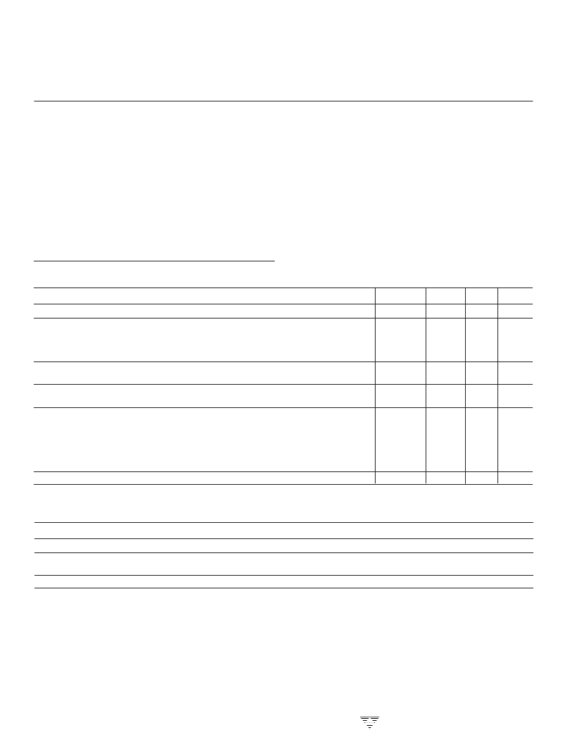
ELECTRICAL CHARACTERISTICS:
T
A
= 25
°
C, unless otherwise specified.
Symbol
Parameter
Test Conditions
V
–
V
IN
=
2.1V
3.0V
4.0V
5.0V
Min
Typ
Max
Unit
V
IN
I
SS
Operating Voltage
Quiescent Current
DET
= 2.1 to 6.0V
1.5
10.0
3.0
3.4
3.8
4.2
(V
–
x 1.02
(V
–
x 0.08
V
1.0
1.3
1.6
2.0
μ
A
V
–
Threshold Voltage
(V
–
x 0.98
(V
–
x 0.02
DET
)
DET
)
V
V
HYST
Hysteresis Range
DET
)
(V
–
x 0.05
7.7
10.1
11.5
13.0
DET
)
DET
)
V
I
OUT
Output Current
Nch V
DS
= 0.5
V
IN
= 2.1V
mA
3.0V
4.0V
5.0V
Pch V
DS
= 2.1V
– 40
°
C
≤
T
A
≤
85
°
C
V
IN
= 8.0V
– 10.0
±
100 ppm/
°
C
T
C
(V
–
)
Tempco of (V
–
)
ABSOLUTE MAXIMUM RATINGS*
Supply Voltage (V
IN).....................................................................
12V
Output Voltage: CMOS ............ (V
SS
– 0.3) to (V
IN
+ 0.3)
Open Drain................. (V
SS
– 0.3) to 12V
Output Current .........................................................50mA
Power Dissipation: (T
A
≤
70
°
C)
SOT-23A-3 .....................................................240mW
SOT-89-3 .......................................................400mW
TO-92
.......................................................440mW
Operating Temperature..........................– 40
°
C to + 85
°
C
Storage Temperature ...........................– 65
°
C to + 150
°
C
Soldering Temperature ...................... 300
°
C, 10 seconds
* Static-sensitive device. Unused devices must be stored in conductive
material. Protect devices from static discharge and static fields. Stresses
above those listed under Absolute Maximum Ratings may cause perma-
nent damage to the device. These are stress ratings only and functional
operation of the device at these or any other conditions above those
indicated in the operational sections of the specifications is not implied.
Exposure to Absolute Maximum Rating Conditions for extended periods
may affect device reliability.
Pin No.
Symbol
Description
1
2
V
IN
V
OUT
Analog input. This pin is both the power supply input and the voltage to be monitored.
Digital output. This output goes low when V
IN
drops below V
high when V
IN
rises above V
–
Ground terminal.
–
and returns
DET
+ V
HYST
. (See timing chart).
3
V
SS
PIN DESCRIPTION
相关PDF资料 |
PDF描述 |
|---|---|
| TC54VN5702EZBSTP | VOLTAGE DETECTOR |
| TC54VN6001ECBRTP | VOLTAGE DETECTOR |
| TC54VN6001ECBSTP | VOLTAGE DETECTOR |
| TC54VN6001EMBRTP | VOLTAGE DETECTOR |
| TC54VN6001EMBSTP | VOLTAGE DETECTOR |
相关代理商/技术参数 |
参数描述 |
|---|---|
| TC54VN5702EZBSTP | 制造商:TELCOM 制造商全称:TelCom Semiconductor, Inc 功能描述:VOLTAGE DETECTOR |
| TC54VN5801ECB | 制造商:TELCOM 制造商全称:TelCom Semiconductor, Inc 功能描述:VOLTAGE DETECTOR |
| TC54VN5801ECBRTP | 制造商:TELCOM 制造商全称:TelCom Semiconductor, Inc 功能描述:VOLTAGE DETECTOR |
| TC54VN5801ECBSTP | 制造商:TELCOM 制造商全称:TelCom Semiconductor, Inc 功能描述:VOLTAGE DETECTOR |
| TC54VN5801EMB | 制造商:TELCOM 制造商全称:TelCom Semiconductor, Inc 功能描述:VOLTAGE DETECTOR |
发布紧急采购,3分钟左右您将得到回复。