- 您现在的位置:买卖IC网 > PDF目录14318 > TC682COA (Microchip Technology)IC REG SWITCHD CAP DBL INV 8SOIC PDF资料下载
参数资料
| 型号: | TC682COA |
| 厂商: | Microchip Technology |
| 文件页数: | 4/14页 |
| 文件大小: | 0K |
| 描述: | IC REG SWITCHD CAP DBL INV 8SOIC |
| 标准包装: | 100 |
| 类型: | 切换式电容器(充电泵),倍增器,反相 |
| 输出类型: | 可调式 |
| 输出数: | 1 |
| 输出电压: | -4.8 V ~ -11 V |
| 输入电压: | 2.4 V ~ 5.5 V |
| 频率 - 开关: | 12kHz |
| 电流 - 输出: | 10mA |
| 同步整流器: | 无 |
| 工作温度: | 0°C ~ 70°C |
| 安装类型: | 表面贴装 |
| 封装/外壳: | 8-SOIC(0.154",3.90mm 宽) |
| 包装: | 管件 |
| 供应商设备封装: | 8-SOICN |
�� �
�
�TC682�
�3.0�
�DETAILED� DESCRIPTION�
�+5V�
�V� IN�
�(+5V)�
�6�
�V� OUT� 4�
�C� 1�
�C� 2�
�+�
�–�
�+�
�–�
�7�
�1�
�2�
�3�
�V� IN�
�C� 1� +�
�C� 1� –�
�TC682�
�C� 2� +�
�C� 2� –�
�V–� OUT�
�+�
�–�
�SW1�
�C� 1�
�SW2�
�SW3�
�+�
�C� 2�
�–�
�SW4�
�-10V�
�–�
�+�
�C� 3�
�V� OUT�
�GND�
�5�
�–�
�+�
�C� OUT�
�R� L�
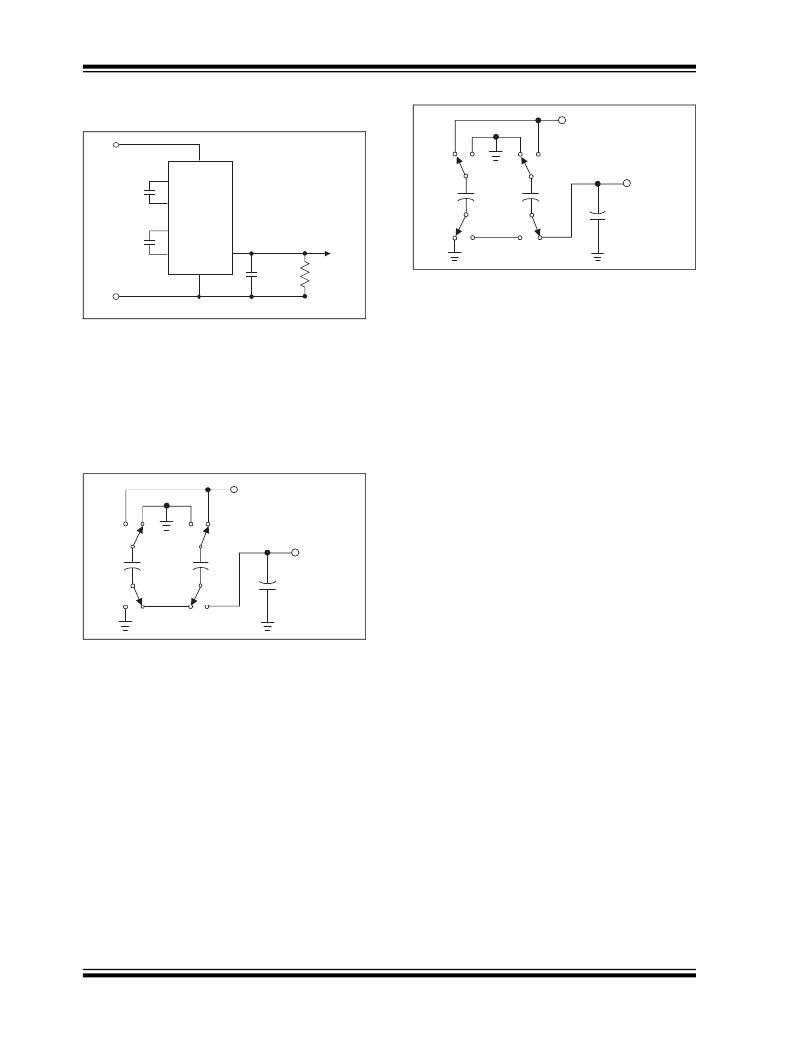
�FIGURE� 3-3:�
�Charge� Pump� –� Phase� 2�
�GND�
�All� Caps� =� 3.3� μ� F�
�3.3�
�Maximum� Operating� Limits�
�FIGURE� 3-1:�
�TC682� Test� Circuit�
�The� TC682� has� on-chip� Zener� diodes� that� clamp� V� IN�
�3.1�
�Phase� 1�
�to� approximately� 5.8V,� and� V� OUT� to� -11.6V.� Never�
�exceed� the� maximum� supply� voltage� or� excessive�
�V� SS� charge� storage� –� before� this� phase� of� the� clock�
�cycle,� capacitor� C� 1� is� already� charged� to� +5V.� C� 1+� is�
�then� switched� to� ground� and� the� charge� in� C� 1–� is�
�transferred� to� C� 2–� .� Since� C� 2+� is� at� +5V,� the� voltage�
�current� will� be� shunted� by� these� diodes,� potentially�
�damaging� the� chip.� The� TC682� will� operate� over� the�
�entire� operating� temperature� range� with� an� input�
�voltage� of� 2V� to� 5.5V.�
�potential� across� capacitor� C� 2� is� now� -10V.�
�3.4�
�Efficiency� Considerations�
�V� IN� =� +5V�
�Theoretically� a� charge� pump� voltage� multiplier� can�
�approach� 100%� efficiency� under� the� following�
�conditions:�
�?� The� charge� pump� switches� have� virtually� no� offset�
�+�
�–�
�SW1�
�C� 1�
�SW2�
�+�
�–�
�SW3�
�C� 2�
�SW4�
�–�
�+�
�C� 3�
�V� OUT�
�and� are� extremely� low� on� resistance.�
�?� Minimal� power� is� consumed� by� the� drive� circuitry.�
�?� The� impedances� of� the� reservoir� and� pump�
�capacitors� are� negligible.�
�-5V�
�For� the� TC682,� efficiency� is� as� shown� below:�
�Voltage� Efficiency� =� V� OUT� /� (-2V� IN� )�
�FIGURE� 3-2:�
�Charge� Pump� –� Phase� 1�
�V� OUT� =� -2V� IN� +� V� DROP�
�V� DROP� =� (I� OUT� )� (R� OUT� )�
�3.2�
�Phase� 2�
�Power� Loss�
�=� I� OUT� (V� DROP� )�
�V� SS� transfer� –� phase� two� of� the� clock� connects� the� neg-�
�ative� terminal� of� C� 2� to� the� negative� side� of� reservoir�
�capacitor� C� 3� and� the� positive� terminal� of� C� 2� to� ground,�
�transferring� the� generated� -10V� to� C� 3� .� Simultaneously,�
�the� positive� side� of� capacitor� C� 1� is� switched� to� +5V� and�
�the� negative� side� is� connected� to� ground.� C� 2� is� then�
�switched� to� V� CC� and� GND� and� Phase� 1� begins� again.�
�DS21453C-page� 4�
�There� will� be� a� substantial� voltage� difference� between�
�V� OUT� and� -2V� IN� if� the� impedances� of� the� pump� capaci-�
�tors� C� 1� and� C� 2� are� high� with� respect� to� their� respective�
�output� loads.�
�Larger� values� of� reservoir� capacitor� C� 3� will� reduce�
�output� ripple.� Larger� values� of� both� pump� and� reservoir�
��“Capacitor� Selection”� “Capacitor� Selection”.�
�?� 2006� Microchip� Technology� Inc.�
�相关PDF资料 |
PDF描述 |
|---|---|
| MAX6712LEXS+T | IC RESET MPU W/RESET SC70-4 |
| GEM36DTAD-S273 | CONN EDGECARD 72POS R/A .156 SLD |
| 382LX272M250B052V | CAP ALUM 2700UF 250V 20% SNAP |
| VI-25D-EX | CONVERTER MOD DC/DC 85V 75W |
| 383LX681M450B052V | CAP ALUM 680UF 450V 20% SNAP |
相关代理商/技术参数 |
参数描述 |
|---|---|
| TC682COA713 | 功能描述:电荷泵 Inverting V Doubler RoHS:否 制造商:Maxim Integrated 功能:Inverting, Step Up 输出电压:- 1.5 V to - 5.5 V, 3 V to 11 V 输出电流:100 mA 电源电流:1 mA 最大工作温度:+ 70 C 封装 / 箱体:SOIC-8 Narrow 封装:Tube |
| TC682CPA | 功能描述:电荷泵 Inverting V Doubler RoHS:否 制造商:Maxim Integrated 功能:Inverting, Step Up 输出电压:- 1.5 V to - 5.5 V, 3 V to 11 V 输出电流:100 mA 电源电流:1 mA 最大工作温度:+ 70 C 封装 / 箱体:SOIC-8 Narrow 封装:Tube |
| TC682EOA | 功能描述:电荷泵 Inverting V Doubler RoHS:否 制造商:Maxim Integrated 功能:Inverting, Step Up 输出电压:- 1.5 V to - 5.5 V, 3 V to 11 V 输出电流:100 mA 电源电流:1 mA 最大工作温度:+ 70 C 封装 / 箱体:SOIC-8 Narrow 封装:Tube |
| TC682EOA713 | 功能描述:电荷泵 Inverting V Doubler RoHS:否 制造商:Maxim Integrated 功能:Inverting, Step Up 输出电压:- 1.5 V to - 5.5 V, 3 V to 11 V 输出电流:100 mA 电源电流:1 mA 最大工作温度:+ 70 C 封装 / 箱体:SOIC-8 Narrow 封装:Tube |
| TC682EPA | 功能描述:电荷泵 Inverting V Doubler RoHS:否 制造商:Maxim Integrated 功能:Inverting, Step Up 输出电压:- 1.5 V to - 5.5 V, 3 V to 11 V 输出电流:100 mA 电源电流:1 mA 最大工作温度:+ 70 C 封装 / 箱体:SOIC-8 Narrow 封装:Tube |
发布紧急采购,3分钟左右您将得到回复。