- 您现在的位置:买卖IC网 > PDF目录98172 > TC7106CLW 1-CH DUAL-SLOPE ADC, PQCC44 PDF资料下载
参数资料
| 型号: | TC7106CLW |
| 元件分类: | ADC |
| 英文描述: | 1-CH DUAL-SLOPE ADC, PQCC44 |
| 封装: | PLASTIC, LCC-44 |
| 文件页数: | 6/26页 |
| 文件大小: | 623K |
| 代理商: | TC7106CLW |
TC7106/A/TC7107/A
DS21455B-page 14
2002 Microchip Technology Inc.
Thedifferential reference canalsobe usedwhenadig-
ital zero reading is required when VIN is not equal to
zero. This is common in temperature measuring instru-
mentation. A compensating offset voltage can be
applied between analog common and VIN-. The trans-
ducer output is connected between VIN+ and analog
common.
The internal voltage reference potential available at
analog common will normally be used to supply the
converter's reference. This potential is stable when-
ever the supply potential is greater than approximately
7V. In applications where an externally generated ref-
erence voltage is desired, refer to Figure 7-1.
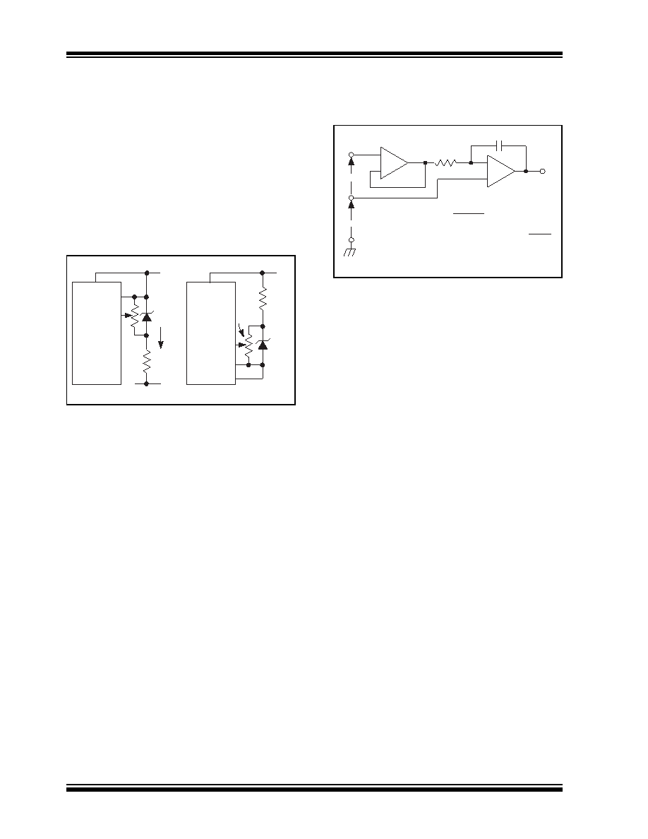
FIGURE 7-1:
EXTERNAL REFERENCE
8.0
DEVICE PIN FUNCTIONAL
DESCRIPTION
8.1
Differential Signal Inputs
VIN+(Pin31), VIN-(Pin 30)
The TC7106A/7017A is designed with true differential
inputs and accepts input signals within the input stage
common mode voltage range (VCM). The typical range
is V+ – 1.0 to V+ + 1V. Common mode voltages are
removed from the system when the TC7106A/
TC7107A operates from a battery or floating power
source (isolated from measured system) and VIN-is
connected to analog common (VCOM) (see Figure 8-2).
In systems where Common mode voltages exist, the
86dB Common mode rejection ratio minimizes error.
Common mode voltages do, however, affect the inte-
grator output level. Integrator output saturation must be
prevented. A worst case condition exists if a large pos-
itive VCM exists in conjunction with a full scale negative
differential signal. The negative signal drives the inte-
grator output positive along with VCM (see Figure 8-1).
For such applications the integrator output swing can
be reduced below the recommended 2.0V full scale
swing. The integrator output will swing within 0.3V of
V+ or V- without increasing linearity errors.
FIGURE 8-1:
COMMON MODE
VOLTAGE REDUCES
AVAILABLE INTEGRATOR
SWING (VCOM ≠ VIN)
8.2
Differential Reference
VREF+(Pin36), VREF-(Pin 35)
The reference voltage can be generated anywhere
within the V+ to V- power supply range.
To prevent rollover type errors being induced by large
Common mode voltages, CREF should be large com-
pared to stray node capacitance.
The TC7106A/TC7107A circuits have a significantly
lower analog common temperature coefficient. This
gives a very stable voltage suitable for use as a refer-
ence. The temperature coefficient of analog common is
20ppm/°C typically.
8.3
Analog Common(Pin32)
The analog common pin is set at a voltage potential
approximately 3.0V below V+. The potential is between
2.7V and 3.35V below V+. Analog common is tied inter-
nally to the N channel FET capable of sinking 20mA.
This FET will hold the common line at 3.0V should an
external load attempt to pull the common line toward
V+. Analog common source current is limited to 10
A.
Analog common is, therefore, easily pulled to a more
negative voltage (i.e., below V+ – 3.0V).
The TC7106A connects the internal VIN+and VIN-
inputs to analog common during the auto-zero cycle.
During the reference integrate phase, VIN- is con-
nected to analog common. If VIN- is not externally con-
nected to analog common, a Common mode voltage
exists. This is rejected by the converter's 86dB Com-
mon mode rejection ratio. In battery operation, analog
common and VIN- are usually connected, removing
Common mode voltage concerns. In systems where V-
is connected to the power supply ground, or to a given
voltage, analog common should be connected to VIN-.
TC7106A
TC7107A
6.8V
Zener
IZ
V+
1.2V
Ref
Common
TC7106A
TC7107A
6.8k
20k
VREF+
VREF-
VREF+
VREF-
(a)(b)
V+
RI
+
–
VIN
VCM
CI
Integrator
VI =
[
VCM – VIN
Input Buffer
CI = Integration Capacitor
RI = Integration Resistor
4000
FOSC
TI = Integration Time =
Where:
VI
–
+
–
+
TI
RI CI
相关PDF资料 |
PDF描述 |
|---|---|
| TC7107AIJL | 1-CH DUAL-SLOPE ADC, CDIP40 |
| TC7106IJL | 1-CH DUAL-SLOPE ADC, CDIP40 |
| TC7107ACLW | 1-CH DUAL-SLOPE ADC, PQCC44 |
| TC7106CKW | 1-CH DUAL-SLOPE ADC, PQFP44 |
| TC7107CKWG | 1-CH DUAL-SLOPE ADC, PQFP44 |
相关代理商/技术参数 |
参数描述 |
|---|---|
| TC7106CLW713 | 功能描述:LCD 驱动器 w/LCD Driver RoHS:否 制造商:Maxim Integrated 数位数量:4.5 片段数量:30 最大时钟频率:19 KHz 工作电源电压:3 V to 3.6 V 最大工作温度:+ 85 C 最小工作温度:- 20 C 封装 / 箱体:PDIP-40 封装:Tube |
| TC7106CPL | 功能描述:LCD 驱动器 w/LCD Driver RoHS:否 制造商:Maxim Integrated 数位数量:4.5 片段数量:30 最大时钟频率:19 KHz 工作电源电压:3 V to 3.6 V 最大工作温度:+ 85 C 最小工作温度:- 20 C 封装 / 箱体:PDIP-40 封装:Tube |
| TC7106CPL | 制造商:Microchip Technology Inc 功能描述:ADC 3-1/2 DIGIT LCD DRIVER 40DIP 制造商:Microchip Technology Inc 功能描述:ADC, 3-1/2 DIGIT, LCD DRIVER, 40DIP 制造商:Microchip Technology Inc 功能描述:ADC, 3-1/2 DIGIT, LCD DRIVER, 40DIP; Resolution (Bits):3.5bit; Supply Current:800A; Digital IC Case Style:DIP; No. of Pins:40; Input Channel Type:Differential; Data Interface:Parallel; Operating Temperature Min:0C; Operating ;RoHS Compliant: Yes |
| TC7106IJL | 功能描述:LCD 驱动器 3-1/2 Digit A/D w/ LCD Driver RoHS:否 制造商:Maxim Integrated 数位数量:4.5 片段数量:30 最大时钟频率:19 KHz 工作电源电压:3 V to 3.6 V 最大工作温度:+ 85 C 最小工作温度:- 20 C 封装 / 箱体:PDIP-40 封装:Tube |
| TC7106IKW | 功能描述:LCD 驱动器 w/LCD Driver RoHS:否 制造商:Maxim Integrated 数位数量:4.5 片段数量:30 最大时钟频率:19 KHz 工作电源电压:3 V to 3.6 V 最大工作温度:+ 85 C 最小工作温度:- 20 C 封装 / 箱体:PDIP-40 封装:Tube |
发布紧急采购,3分钟左右您将得到回复。